Is this map of S-CPU address space accurate? Is it useful?
Keywords for search: snes memory map
Other than the weirdness where there's two rows for the SFRs in banks $80-$BF but only one in banks $00-$3F, it looks good?
I find myself wondering whether it would be any "better" if you didn't represent 1KiB per tile but instead just 256 bytes, for a 1056x1088 image instead. Probably not...
lidnariq wrote:
Other than the weirdness where there's two rows for the SFRs in banks $80-$BF but only one in banks $00-$3F, it looks good?
Where did the name "SFRs" come from? I know them as "MMIO areas". Corrected below.
Anyone know what the standard battery RAM addresses are in LoROM and HiROM?
SFR ("special function register") is microcontroller (at least PIC and 8051) jargon.
Nocash's fullsnes claims that
LoROM puts save RAM in banks $70-$7D and $F0-$FF, either just the lower half (pages $00-$7F) or the entire 64 KiB, and that HiROM puts save RAM in a whole slew of different places, always pages $60-$7F, most often banks $20-$3F and $A0-$BF, but sometimes banks $1x, $3x, $9x, and $Bx; or banks $80-$BF.
lidnariq wrote:
Nocash's fullsnes claims that
LoROM puts save RAM in banks $70-$7D and $F0-$FF, either just the lower half (pages $00-$7F) or the entire 64 KiB, and that HiROM puts save RAM in a whole slew of different places, always pages $60-$7F, most often banks $20-$3F and $A0-$BF, but sometimes banks $1x, $3x, $9x, and $Bx; or banks $80-$BF.
There are dozens of board layouts that place cartridge ROM and RAM in different places, and sometimes have certain areas be open bus.
Categorizing SNES mapping as "LoROM" or "HiROM" is like rounding pi to 3. It'll give you the gist of it, but don't bother trying to use it for anything serious.
You can find specific board layouts here:
http://code.google.com/p/higan/source/b ... Boards.bml
It might help to put some small text on the graphic itself. Maybe a simple web page with some radio buttons for which mode is in use could let it be not too cluttered.
In
this post, koitsu asked why $0000 is at the top. I drew it that way because $0000 is also at the top of a hex dump, such as that shown in a debugging emulator's memory viewer.
It has come to my attention that splitting the information into several files would explain things better than trying to cram it into one. So I made one overview map for what the S-CPU sees and one for each common mapping (LoROM and HiROM).
Attachment:
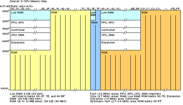 snes overall memory map.png [ 3.45 KiB | Viewed 7643 times ]
Attachment:
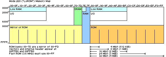 snes lorom memory map.png [ 2.31 KiB | Viewed 7643 times ]
Attachment:
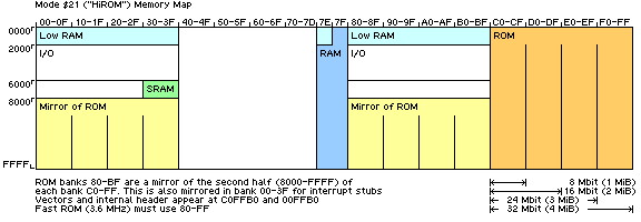 snes hirom memory map.png [ 2.51 KiB | Viewed 7643 times ]
Cool, that looks a lot better than the old image. I like the text now being shown directly inside of the map, and bank numbers above the map, and less footnotes, and less small boxes, etc.
Shouldn't the HiROM map also show ROM (mirror) in bank 40-7Dh? I don't know if/how many games use that area for ROM, but I would have thought that ROM is mapped/mirrored there in most cartridges (of course ROM is usually also mirrored here and there, and it wouldn't be helpful to show all of those mirrors - because they are rather unwanted dirt effects than actually used memory areas).
Maybe it would make sense to add a headline saying "Banks" above of the 00-FF values, and something similar saying "Offset" for 0-FFFF. And something pointing out that 8bit:16bit "Bank:Offset" can be also expressed as 24bit "Address". But if the images are used on wiki/webpage, then that could be explained in the page text, not in the image.
Anyways, it's probably better to keep it simple (or even a bit simplified) without too many details.
nocash wrote:
Shouldn't the HiROM map also show ROM (mirror) in bank 40-7Dh?
The board puts it there, but I don't really think game programmers were meant to use it there. It's not like the $80-$BF mirrors, which are good for having half a bank of ROM in the same data bank as low RAM and I/O, or the mirror at $00, which is good for interrupt stubs that
jml to the real handler in fast ROM. It's just another copy of the ROM sitting there in the slow area. Further, if a game gets upgraded to mode $25 ("ExHiROM"), reliance on $40-$7D and $80-$FD carrying the same data would break. So HiROM's mirror in $40-$7D might be considered what you call a "dirt effect".
What about HiROM boards that used SlowROM chips? Seems to me they'd have to use the lower mapping, right?
According to
Fullsnes section "SNES Memory Control", the top half of ROM address space can be switched between 2.7 MHz and 3.6 MHz modes.
MEMSEL ($420D; corresponds to WAITCNT in Game Boy Advance and EXMEMCNT in Nintendo DS)
Write 0 for slow ROM in $80-$FF or 1 for fast ROM in $80-$FF
My init code sets MEMSEL based on the cartridge header:
Code:
MEMSEL = $80420D
map_mode = $00FFD5
; ...
lda f:map_mode
and #$10
beq not_fastrom
inc a
not_fastrom:
sta MEMSEL
(An immediate load would be smaller, but I'm intentionally sacrificing 7 bytes for clarity and the
single source of truth principle in this demo.)
Ah ok, great, I get it now.
Though I wonder why in the manual they specify the Mode 20 ROM area to be in the SlowROM banks, and the mirrored ROM to be in the upper banks instead of the other way around, if the upper banks can do fast or slow speeds.
probably because it best and less confusing if you think of the lower mapping as always slow and the upper as always fast, even though this is not the case, and you can make the upper slow if you want. But this then forms a hard rule. lower mapping always slow, upper mapping "fast"
if you are in the lower banks it will always be slow and thus it won't fail, in that if MEMSEL gets the wrong value somehow, it will still be slow access and your cart will work.