tepples wrote:
Yet the Sony design continues to show through, as VAG is BRR with a longer packet, different filter types, and a different Gaussian table.
Interesting. And unexpected. Does it seem to match-up with PSX adpcm samples (16-byte PSX blocks, instead of 9-byte SNES blocks)?
And did you see further differences, like more channels or whatever? There should be some way to switch to SNES-compatible mode; either via APU registers, or maybe via 21E4h.
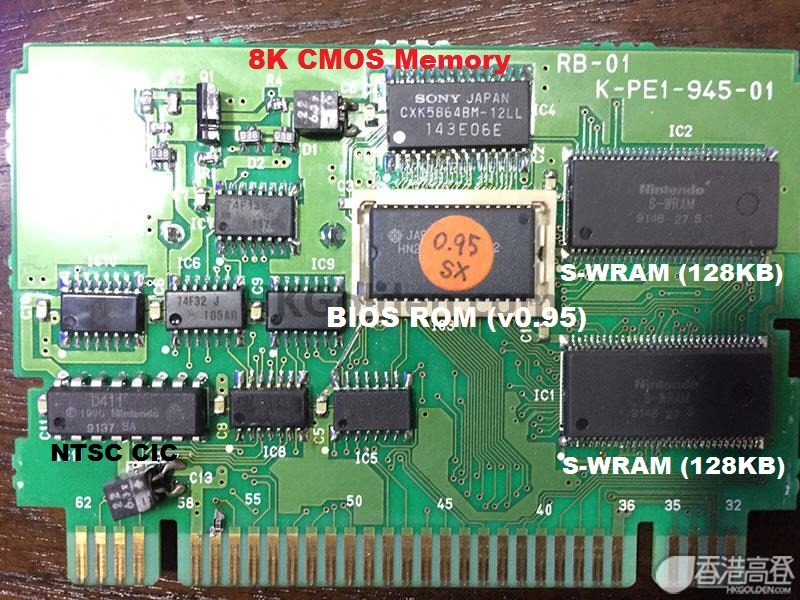
The mainboard photos are in fact showing uncommon part numbers for both APU chips (so even the SPC700 CPU might be a bit different, it's clearly running SPC700 code though).
One weird thing is that the new APU couldn't be used in CDROM expansions (for existing SNES consoles), unless it where mapped to some other 21xxh addresses in case of expansion models.
byuu wrote:
$21e4 is the interrupt enable (d3 = NEC CPU, d2 = Sony CPU.)
$21e0 and $21e5 are unknown still.
We need to return "10100" from the status register for the BIOS to think there's a data CD present. Or "11000" for a music CD. I don't know what other values will work or not work.
Also, there's a nice datasheet on the CXD1803AQ that may be similar to the CXD1800Q.
I didn't track down 21E4h bits yet, but yes, it should be probably something for disabling the new interrupts (or even disabling the whole new I/O ports for backwards compatibility with normal SNES carts).
21D0h, 21E0h, 21E5h seem to locking/unlocking the battery backed SRAM (ie. located in the BIOS cartridge, not related to the CDROM hardware).
The 5-digit status can be set to various values. The first two digits set to 00h or FFh switches between "Music Disc" and "Press Start" (for data discs). The middle digit set to 1..4 or so works, but bigger values give "Not Defined", 0 gives No Disc. In some cases, the middle digit seems to be ignored depending on first 2 digits though. The last two digits seem to have no effect on anything. Best might be to watch the status values on real hardware (if it would work), and check if how they are changing on inserting/ejecting different discs, and on sending different mechacon commands.
Why CXD1803AQ? Guess you missed the note about the CXD1196AR datasheet - it looks almost perfectly right to me (the only difference that I've spotted yet is related to some Test register, I haven't compared it to closely against the test screens yet though).
I've ported the relevant datasheet section to txt (see below). Some of sentences in there are really obfuscated (overcomplicated long sentences, formatted at 120-column width, and refusing to use terms like "0" and "1"). I am working on reversing what they wanted to say in that document. As by now, it's looking as if it'd be quite easy to emulate (when not emulating any read errors).
The biggest problem might be the user interface for loading cdrom images, and supporting all of the numerous different cdrom image formats (I might be able to clean-up the cdrom code from no$psx for re-using it in no$sns; oh, and I think other emu programmers completely got around cdrom-image decoding by simply prompting users to mount the cdrom image as virtual cdrom drive via external utilities).
Code:
CXD1196AR - Write register
---------------------------
REG A0 RA bit7 bit6 bit5 bit4 bit3 bit2 bit1 bit0
REGADR L X L L L RA4 RA3 RA2 RA1 RA0
RESERVED H X0 L L L L L L L L
DRVIF H X1 XSLOW C2PO L1st LCH LOW BCK RED BCK MD1 BCK MD0 LSB 1st CLKL
CHPCTL H X2 L L CLR ADP CHP RST CDDA SW OPEN RPSTART ADP EN
DECCTL H X3 AUTO CI L MODE SEL FORM SEL AUTODIST DEC MD2 DEC MD1 DEC MD0
INTMSK H X4 ADP END DEC TOUT DMA CMP DEC INT CI ERR L L L
INTCLR H X5 ADP END DEC TOUT DMA CMP DEC INT CI ERR L L L
CI H X6 L EMPH ASIS L BIT L4H8 L FS L3H1 L MONO STE
DMA ADRC-L H X7 bit7 bit6 bit5 bit4 bit3 bit2 bit1 bit0
DMA ADRC-H H X8 L bit14 bit13 bit12 bit11 bit10 bit9 bit8
DMA XFRC-L H X9 bit7 bit6 bit5 bit4 bit3 bit2 bit1 bit0
DMACTL H XA xfrc11 xfrc10 xfrc9 xfrc8 DMA EN L L L
DRV ADRC-L H XB bit7 bit6 bit5 bit4 bit3 bit2 bit1 bit0
DRV ADRC-H H XC L bit14 bit13 bit12 bit11 bit10 bit9 bit8
TEST2 H 1D L L L L L L L L
TEST1 H 1E L L L L L L L L
TEST0 H 1F L L L L L L L L
Write Registers
2.1.1 Register address (REGADR) register
This register is used for selection of the internal registers.
(1) When A0 = XCS = `L', the REGADR register is selected. When A0 = `H' and XCS = `L', the register
specified by the REGADR is selected.
(2) When the low order 4 bits of REGADR are not 0 (hex), and a register write or read is made by setting
A0 = `H' and XCS = `L', the low order 4 bits of REGADR are incremented.
(3) REGADR is cleared by rising edge of DMAEN bit (bit3) of the DMACTL register. (Cleared to 00 (hex).)
2.1.2 DRIVE Interface (DRVIF) register
Bit7 XSLOW (/SLOW SPEED)
`H' : A DMA cycle is performed in 4 clocks.
In this case, a standard SRAM with an access time of less than 120 nsec can be connected
to the CXD1196AR.
`L' : A DMA cycle is performed in 12 clocks. When the CXD1196R is connected to an SRAM
with a slower access time, set this bit at `L'. In this case, a standard SRAM with an access
time of less than 320 ns can be connected to the CXD1196AR. For operation at VDD = 3.5
V, set this bit to L.
Bit6 C2PL1ST (C2PO Ler-byte 1st)
`H' : To input two bytes of DATA input, each with a C2PO identifying the lower or upper byte, in
the order of the lower and upper bytes
`L' : To input two bytes of DATA input, each with a C2PO identifying the upper or lower byte, in
the order of the upper and lower bytes.
Here, the upper byte means the 8 (eight) upper bits including the MSB from the DSP for CD. And the lower
byte means the 8 (eight) lower bits including the LSB from the DSP for CD. For example, the minute byte
of the Header is a lower byte and the sec byte is a upper byte.
Bit5 LCHLOW (LCH LOW)
`H' : To determine that the data is Lch data when LRCK = `L'
`L' : To determine that the data is Lch data when LRCK = `H'
Bit4 BCKRED (BCLK Rising Edge)
`H' : To strobe DATA by the rising edge of BCLK
`L' : To strobe DATA by the falling edge of BCLK
Bit3, 2 BCKMD1, 0 (BCLK Mode 1, 0)
Set these bits, depending on the number of BCLK clocks output by the DSP for CD during a cycle of
WCLK.
BCKMD1 BCKMD0
`L' `L' 16BCLKs/WCLK
`L' `H' 24BCLKs/WCLK
`H' `X' 32BCLKs/WCLK
Bit1 LSB 1ST (LSB First)
`H' : To connect to a DSP for CD which outputs DATA on an LSB first basis
`L' : To connect to a DSP for CD which outputs DATA on an MSB first basis
Bit0 CLKLOW (CLK LOW)
`H' : To fix CLK pin output at `L'
`L' : To output 8.4672 MHz clock from CLK pin output
The values of the individual bits of this register must be changed with the decoder in the disabled state.
Table 2.1.1 shows the values of bits of bit 6 through 1 to be set when the CXD1196AR is connected to
Sony DSPs for CD. Fig. 2.2.1 (1) through (3) show input timing charts.
DRVIF register
Sony DSP for CD bit6 bit5 bit4 bit3 bit2 bit1 Timing chart
-----------------------------------------------------------------------------
CDL30 series L L L L H L Fig. 2.1.1 (1)
CDL35 series
-----------------------------------------------------------------------------
CDL40 series L L H L H L Fig. 2.1.1 (2)
(48-bit slot mode)
-----------------------------------------------------------------------------
CDL40 series L H L H X H Fig. 2.1.1 (3)
(64-bit slot mode)
Table 2.1.1 DRVIF Register Settings
(Note 1)
CDL30 series: CXD1125Q/QZ, CXD1130Q/QZ, CXD1135Q/QZ,
CXD1241Q/QZ, CXD1245Q, CXD1246Q/QZ,
CXD1247Q/QZ/R, etc.
CDL35 series CXD1165Q, CXD1167Q/QZ/R, etc.
CDL40 series CXD2500Q/QZ, etc.
2.1.3 Chip Control (CHPCTL) register
Bit7-5 RESERVED
Bit4 CHPRST (Chip Reset)
When this bit is set at `H', the CXD1196AR is internally initialized. The bit setting will automatically
change to `L' when the internal initialization of the CXD1196AR is completed. Therefore, there is no
need for the CPU to change the setting at `L'. Initialization of the CXD1196AR will be completed in
500ns after the bit has been set at `H' by the CPU.
Bit3 CD-DA (CD-Digital Audio)
`H' : When a CD-DA disc is to be played back, this bit is set at `H'.
The decoder must be placed in the disabled state (DECCTL register) when this bit is set at
`H'.
`L' : When a CD-ROM disc is to be played back, this bit is set at `L'.
Bit2 SWOPN (Sync Window Open)
`H' : When this bit is set at `H', the window for detection of SYNC mark will open. In this case,
the SYNC protection circuit in the CXD1196AR will be disabled.
`L' : When this bit is set at `L', the window for detection of SYNC mark will be controlled by the
SYNC protection circuit in the CXD1196AR.
Bit1 RPSTART (Repeat Correction Start)
When the DECODER is placed in the repeat correction mode, and this bit set at `H', the error
correction of the current sector will begin. The bit setting will automatically change to `L' when
correction begins. Therefore, there is no need for the CPU to change the setting at `L'.
Bit0 ADPEN (ADPCM Enable)
When the current sector is an ADPCM sector, the CPU sets this bit at `H' in less than 11.5 ms after a
decoder interrupt (DECINT). When the current sector is not an ADPCM sector, the CPU changes the
bit setting at `L' in less than 11.5 ms after a decoder interrupt (DECINT).
2.1.4 DECODER CONTROL (DECCTL) Register
Bit7 AUTOCI (Auto Coding Information)
`H' : To perform ADPCM playback according to the coding information from the drive. In this
case, the CI register need not be set.
`L' : To perform ADPCM playback according to the value of the CI register.
Bit6 RESERVED
Should be kept at `L' at all times.
Bit5 MODESEL (Mode Select)
Bit4 FORMSEL (Form Select)
When AUTODIST = `L', the sector is corrected as the following MODE and FORM.
MODESEL FORMSEL
`L' `L' MODE1
`H' `L' MODE2, FORM1
`H' `L' MODE2, FORM2
Bit3 AUTODIST (Auto Distinction)
`H' : Errors are corrected according to the MODE byte and FORM bit read from the drive.
`L' : Errors are corrected according to bit 5 MODESEL and bit4 FORMSEL.
Bit2-0 : DECMD 2-0 (Decoder Mode 2-0)
DECMD2 DECMD1 DECMD0
`L' `L' `X' Decoder disable
`L' `H' `X' Monitor only mode
`H' `L' `L' Write only mode
`H' `L' `H' Real time correction mode
`H' `H' `L' Repeat correction mode
`H' `H' `H' Inhibit
These bits are set at `L' when the CDDA bit (bit3) of the CHPCTL register is `H'.
2.1.5 Interrupt Mask (INTMSK) Register
When the individual bits of this register are set at `H', an interrupt request from the CXD1196AR to the CPU
is enabled in response to the corresponding interrupt status. (That is, when the interrupt status is created,
the INT pin is made active.) The value of the individual bits of the register does not affect the
corresponding interrupt status.
Bit7 ADPEND (ADPCM End)
When this chip has completed the ADPCM decode for a sector, if the ADPCM decode for the next
sector is not enabled, the ADPEND status is created.
Bit6 DECTOUT (Decoder Time Out)
If no SYNC mark is detected during a period of 3 sectors (40.6 ms in normal speed playback mode)
after the DECODER has been set in the monitor only, and real time correction modes, the DECTOUT
status is created.
Bit5 DMACMP (DMA Complete)
When DMA is ended by DMAXFRC, the DMACMP status is created.
Bit4 DECINT (Decoder Interrupt)
If a SYNC mark is detected or internally inserted during execution of the write only, monitor only and
real time correction modes by the DECODER, the DECINT status is created. When the SYNC mark
detected window is open, however, if the SYNC mark spacing is less than 2352 bytes, the DECINT
status is not created. During execution of the repeat correction mode by the DECODER, the
DECINT status is created each time a correction ends.
Bit3 CIERR (Coding Information Error)
When AUTOCI bit of DECCTL register is set at "H" and ADPCM decode playback is done, if there is
an error in a CI byte of an ADPCM sector, the CIERR status is created. ADPCM decode playback of
this sector will not be done.
Bit2-0 RESERVED
2.1.6 Clear Interrupt Status (INCTCLR) Register (uh, "INCT", not INT?)
When the individual bit of this register is set at `H', the corresponding interrupt status is cleared. The
individual bit is automatically set at `L' after the interrupt status has been cleared. Therefore, there is no
need for the CPU to change the setting at `L'.
Bit7 ADPEND (ADPCM End)
Bit6 DECTOUT (DECODER Time Out)
Bit5 DMACMP (DMA Complete)
Bit4 DECINT (DECODER Interrupt)
Bit3 CIERR (Coding Information Error)
Bit2-0 RESERVED
2.1.7 Coding Information (CI) Register
When ADPCM decoding is to be done by setting AUTOCI = `L', the coding information is written to this
register. The bit configuration is the same as that of the coding information byte of the sub header.
2.1.8 DMA Address Counter-L (DMAADRC-L)
2.1.9 DMA Address Counter-H (DMAADRC-H)
This counter retains the address to be used by the CPU when reading data from the buffer. When the data
to be sent to the CPU is read from the buffer, the contents of the DMAADRC are output from MA0-14.
Each time data to be sent to the CPU is read from the buffer, the DMAADRC is incremented.
The CPU sets the head address of DMA in the DMAADRC before starting DMA. The CPU can read and
set the contents of the DMAADRC at any time. Do not change the contents of the DMAADRC during
execution of DMA.
2.1.10 DMAXFRC-L
2.1.11 DMA Control (DMACTL) register
Bit7 DMAXFRC11 Bit11 (MSB) of DMAXFRC (Transfer Counter)
Bit6 DMAXFRC10 bit10 of DMAXFRC
Bit5 DMAXFRC9 bit9 of DMAXFRC
Bit4 DMAXFRC8 bit8 of DMAXFRC
Bit3 DMAEN (CPU DMA Enable)
`H' : To enable DMA
`L' : To inhibit DMA
Bit2-0 RESERVED
The DMAXFRC (DMA Transfer Counter) is a counter which indicates the number of DMA transfers. Each
time the data to be transferred to the CPU is read from the buffer, the counter is decremented. When the
value of the DMAXFRC reaches 0, DMA ends. At this point, interrupt request may be output to the CPU.
When data transfer is not to be ended by DMAXFRC as in the case of data transfer in the I/O mode,
DMAXFRC should be set at 0 when data transfer is started (when DMAEN bit is set at `H'). The CPU can
read and set the contents of DMAXFRC at any time. During execution of DMA, do not change the contents
of DMAXFRC.
2.1.12 DRVADRC-L (Drive Address Counter-L)
2.1.13 DRVADRC-H
The DRVADRC is a counter which retains the address for writing the data from the drive to the buffer.
When the drive data is written to the buffer, the value of DRVADRC is output from MA01-14 pins. Each
time a byte of data from the drive is written to the buffer, the DRVADRC is incremented.
Before execution of the write only mode and real time correction mode of the DECODER, the CPU sets the
buffer write head address in the DRVADRC.
The CPU can read and set the contents of DRVADRC at any time. During execution of DMA, do not
change the contents of DRVADRC.
CXD1196AR - Read register
----------------------------
REG A0 RA bit7 bit6 bit5 bit4 bit3 bit2 bit1 bit0
REGADR L X X X X RA4 RA3 RA2 RA1 RA0
DMA DATA H 00 bit7 bit6 bit5 bit4 bit3 bit2 bit1 bit0
INTSTS H 01 ADP END DEC TOUT DMA CMP DEC INT CI ERR X X X
STS H 02 DRQ ADP BSY ERIN BLK COR INH EDC OK ECC OK SHRT SCT NO SYNC
HDRFLG H 03 MIN SEC BLO CK MODE FILE CHAN NEL SUB MODE CI
HDR MIN H X4 bit7 bit6 bit5 bit4 bit3 bit2 bit1 bit0
HDR SEC H X5 bit7 bit6 bit5 bit4 bit3 bit2 bit1 bit0
HDR BLOCK H X6 bit7 bit6 bit5 bit4 bit3 bit2 bit1 bit0
HDR MODE H X7 bit7 bit6 bit5 bit4 bit3 bit2 bit1 bit0
SHDR FILE H 08 bit7 bit6 bit5 bit4 bit3 bit2 bit1 bit0
SHDR CH H 09 bit7 bit6 bit5 bit4 bit3 bit2 bit1 bit0
SHDR S-MODE H 0A bit7 bit6 bit5 bit4 bit3 bit2 bit1 bit0
SHDR CI H 0B bit7 bit6 bit5 bit4 bit3 bit2 bit1 bit0
CMADR L H 0C bit7 bit6 bit5 bit4 bit3 bit2 bit1 bit0
CMADR H H 0D X bit14 bit13 bit12 bit11 bit10 bit9 bit8
MDFM H XE X X X RAW MD2 RAW MD1 RAW MD0 C MODE C FORM
ADPCI H XF MUTE EMPHASIS EOR BIT L4H8 X FS L3H1 X MONO STE
DMA XFRC-L H 18 bit7 bit6 bit5 bit4 bit3 bit2 bit1 bit0
DMA XFRC-H H 19 X bit14 bit13 bit12 bit11 bit10 bit9 bit8
DMA ADRC-L H 1A bit7 bit6 bit5 bit4 bit3 bit2 bit1 bit0
DMA ADRC-H H 1B X bit14 bit13 bit12 bit11 bit10 bit9 bit8
DRV ADRC-L H 1C bit7 bit6 bit5 bit4 bit3 bit2 bit1 bit0
DRV ADRC-H H 1D X bit14 bit13 bit12 bit11 bit10 bit9 bit8
TEST 0 to 2 H 10 to 2 X X X X X X X X
Read Registers
In the descriptions of the registers STS, HDRFLG, HDR, SHDR and CMADR, what is referred to as the
current sector refers to the sector where registers are valid for a decoder interrupt (DECINT). In the monitor
only and write only modes, the sector from the DSP for CD just before a decoder interrupt is called the
current sector. In the real time correction mode and repeat correction mode, the sector that has gone
through error detection and correction is referred to as the current sector.
2.2.1 Register Address (REGADR) Register
2.2.2 DMADATA Register
When data transfer (buffer read) is to be made in the I/O mode, the CPU reads data from this register.
2.2.3 Interrupt Status (INTSTS) Register
The values of the individual bits of this register indicate the respective associated values of interrupt status.
These bits are not affected by the values of the individual bits of the INTMSK register.
Bit7 ADPEND (ADPCM End)
Bit6 DECTOUT (DECODER Time Out)
Bit5 DMACMP (DMA Complete)
Bit4 DECINT (DECODER Interrupt)
Bit3 CIERR (Coding Information Error)
2.2.4 Status (STS) Register
Bit7 DRQ (Data Request)
This bit indicates the value of the DRQ pin.
Bit6 ADPBSY (ADPCM BUSY)
This bit goes `H' during ADPCM playback.
Bit5 ERINBLK (Erasure in Block)
On all the bytes of the current sector except the SYNC byte, this bit goes `H' if there is one or more
bytes from the DSP for CD whose C2 pointer is ON.
Bit4 CORINH (Correction Inhibit)
When the DECCTL register is set AUTODIST bit = `H', this bit goes `H' if the error flag is ON in the
MODE (and FORM) byte.
Bit3 EDCOK
Indicates EDC check showed there were no errors in the current sector.
Bit2 ECCOK
Indicates there are no more errors from the Header to P parity bytes in the current sector. (In the
MODE2, FORM2 sector, this bit is treated as a DON'T CARE bit.)
Bit1 SHRTSCT (Short Sector)
Indicates the Sync Mark interval was less than 2351 bytes. On this sector, neither ECC nor EDC is
executed.
Bit0 NOSYNC
Indicates that the SYNC Mark, not detected in the predetermined position, is one internally inserted.
2.2.5 Header Flag (HDRFLG) Register
Indicates the value of the error pointer of the Header and Sub Header registers.
2.2.6 Header (HDR) Register
It is a 4-byte register indicating the Header byte of the current sector. The CPU can find the value of the
Header byte of the current sector from the Minute byte as it sets the REGADR register at X4 hex and
successively reads data.
2.2.7 Sub Header (SHDR) Register
It is a 4-byte register indicating the Sub Header byte of the current sector. The CPU can find the value of
the Sub Header byte of the current sector from the File byte as it sets the REGADR register at 08 hex and
successively reads data.
2.2.8 Current Minute Address L (CMADR-L) Register
2.2.9 Current Minute Address H (CMADR-H) Register
Indicates the buffer memory address where the Minute bytes of the current sector (after correction) is in
store.
2.2.10 MODE/FORM (MDFM) Register
Bit4-2 RMODE2-0
RMODE2 : Indicates the logic sum of the value of the high-order 6 bits of the raw MODE byte and the
pointer.
RMODE1, 0 : Respectively indicate the values of the low-order 2 bits of the raw MODE byte.
Bit1 CMODE (Correction Mode)
Bit0 CFORM (Correction Form)
These bits indicate which of the MODEs and FORMs this IC determined that the current sector was
associated with when it corrected errors.
CFORM CMODE
`X' `L' MODE1
`L' `H' MODE2, FORM1
`H' `H' MODE2, FORM2
2.2.11 ADPCI (ADPCM Coding Information) Register
Bit7 MUTE
This bit goes `H' when the DA data is muted on.
Bit6 EMPHASIS
This bit goes `H' when the ADPCM data is emphasized.
Bit5 EOR (End of Record)
This bit goes `H' when the Sub Mode byte bit0 = `H' and there is no error in the Sub Mode byte.
Bit4 BITLNGTH (Bit Length)
This bit indicates the bit length of ADPCM playback coding information.
`H' : 8 bits
`L' : 4 bits
Bit2 FS (Sampling Frequency)
This bit indicates the ADPCM playback sampling frequency.
`H' : 18.9 kHz
`L' : 37.8 kHz
Bit0 M/S (MONO/STEREO)
This bit indicates "monaural" or "stereo" of ADPCM playback coding information.
`H' : Stereo
`L' : Monaural
2.2.12 DMAXFRC-L
2.2.13 DMAXFRC-H
2.2.14 DMAADRC-H ;uh, "-H", not "-L"?
2.2.15 DMAADRC-H
2.2.16 DRVADRC-L
2.2.17 DRVADRC-H
