I wanted to try and RE the CIC, but have found little info on it. I know some guys were trying to get the source code using an electron microscope. I'd rather not go this route because it would be no different than getting the source from the patent like tengen did. Has any one ever tried to data log the communications between the key and lock? Maybe we could lower the clock speed to make it easier to log. This is just speculation on how I think it could work. I'm thinking that the Lock sends a number to the Key, then they both use this as the seed for some alogarithim or random number generator. After so many clock cycles the key sends it's results to the lock. The lock then compares it with what it calculated and responds accordingly. Does this sound feasible? Or am I way off track. Not having a CIC replacement is one of our biggest barriers in developing new games, so we need to crack this thing. Any suggestion would be greatly appreciated.
My understanding is that the two CIC chips run identical programs and continually communicate some portion of their state between each other. If these communications differ, the NES goes into reset mode. I heard that someone once tried to log these communications, but even after hundreds of megabytes of data there was no repetition.
The electron microscope route to uncover the source code would not ultimately be to merely copy the source code, but to reverse-engineer it and write new code (for something more modern like a PIC microcontroller) that gives the same result as the original CIC code.
It's funny that modern encryption schemes like CSS and the like have been broken, but this ancient copy protection chip is still a mystery.
Something to look into.. Has patent protection expired on this? It must have been more than 20 years since the patents were filed. Not knowing much about these things, I would expect the patent protection to last for about 15 years. If the protection has expired, then perhaps it wouldn't be necessary to be selective in your methods.
I'm not against the SEM I just want to take a different approach.
Perhaps whoever tried datalogging it either wasn't thorough or maybe this thing needs a different approach. What if we just take a small sample and then try to find alogarithms that will produce the same output. It probably wouldn't take much to narrow down one that is the same. Assuming it is a 4bit MPU and we know for sure it's clock is 4Mhz. It can only perform so many operations. It probably transfers 1 or more nibbles at a time. For each nibble added the possibilites increase but it also reduces the amount of operations it can perform on it. When you take into account the 1hz square wave it outputs for reset. That only leaves 1s to apply an alogarithm. Not to mention the MPU probably takes multiple clock cycles per instruction. Any ideas on making a 2bit data logger?
Perhaps whoever tried datalogging it either wasn't thorough or maybe this thing needs a different approach. What if we just take a small sample and then try to find alogarithms that will produce the same output. It probably wouldn't take much to narrow down one that is the same. Assuming it is a 4bit MPU and we know for sure it's clock is 4Mhz. It can only perform so many operations. It probably transfers 1 or more nibbles at a time. For each nibble added the possibilites increase but it also reduces the amount of operations it can perform on it. When you take into account the 1hz square wave it outputs for reset. That only leaves 1s to apply an alogarithm. Not to mention the MPU probably takes multiple clock cycles per instruction. Any ideas on making a 2bit data logger?
Such a data logger has already been made by kevtris, and the data stream is extremely sparse - short bursts of '1' (each 3 clocks long) followed by huge spans of '0' (ranging from 76 to well over ten thousand).
Note that the CIC is clocked at 4MHz, but the clock is effectively divided by 4, resulting in two 1MHz data streams.
Note that the CIC is clocked at 4MHz, but the clock is effectively divided by 4, resulting in two 1MHz data streams.
If you write your own original program that performs the same function, then you are not violating the copyright, but you may be violating the patent. The patent has expired (filing + 20), but the copyright has not.
The biggest obstacle to CIC RE right now is the unknown 1. instruction set architecture and 2. layout of addresses in the internal ROM.
The biggest obstacle to CIC RE right now is the unknown 1. instruction set architecture and 2. layout of addresses in the internal ROM.
I dont think looking at the data stream is the solution, mainly because I have tried and failed =] Atari/Tengen also tried and failed. They eventually decapped the chip. I am waiting for ~6 more lockout chip versions to be decapped from neviksti, the same guy that did the other one on cherryroms. I am hoping the roms from all of them can be compared to get more architecture info. So far none of the permutations/inversions of the rom data match any Sharp instruction sets I have found.
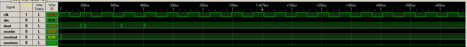
If you want to look at the stream there is some important starting information. First is the bit rate is not as described on the patent info. This will be shown in the picts below. Second is there are only 16 unique streams, selected by the cic chip in the nes at the beginning. Each stream is apparently non repeating and constant, so record/playback is not an option. The data stream is very sparse with long and VERY long pauses between pulses.
Here is what I have learned so far, gathered from a usa nes-cpu-11 + logic analyzer. I connected directly to the cic in the nes, so dout is to cart and din is from cart. Ignore clock in all pictures except for the close up of the pulse. The first transaction syncs the chips using resetout line from nes->cart. Then the nes selects 1 of 16 streams, shown in the first 4 pulses. The length and pause between those pulses is shown close up. The clock does not seem to match the patents. After that the bits transferred are always the same, and resetnes goes high when the cart is authenticated ~1300uS later. When there is no cart, some bits are missing and resetnes stays low and starts the 1hz sequence. Now comes the sparse part. There is nothing for ~2.5mS, then a second transaction. All 16 possible second transactions are shown. I was hoping it was send 16 bits, wait 2.5mS, send 16 bits, etc but that doesnt line up later. The data transfers just keep going and are similarly sparse. Disconnecting either din or dout at any time causes it to go into reset so both chips are still looking for input from the other.
If I ever get some more free time I can capture more sequences, and also look at the protocol of the other country lockouts. I am guessing the other country ones just switch around what number each stream is.
tepples wrote:
The biggest obstacle to CIC RE right now is the unknown 1. instruction set architecture and 2. layout of addresses in the internal ROM.
I agree, and I think the unknown ISA is the biggest of the problems. Using Nevitski's pictures I have transcoded the binary for the code. However, this is useless without knowing the instruction set. I haven't gone so far as to try to map it to the Sharp chips, but it looks like bunnyboy has done so. If there are any crypto experts out there that could take the info we have and turn it into a number crunching excercise that would be great. I'm sure we can round up enough cpu cycles to solve it, the problem is framing the question so that this approach can be tried.
Thanks for all the info above. It should save me considerable time. I'm glad to see that I'm not the only one bothered by this unsolved mystery.
I pulled a couple CIC's off some carts and stuck them in a bread board. I don't have a logic probe so I'm just going to use the parallel port on my computer. I did some experiments and found that they still function @ 100Khz clock speed.
Do you think that the Lock selecting one of the 16 streams is the seed for the key to use as a number generator? If so than maybe analyzing all the streams together would make cracking the code easier.
I read the cherryrom forum about extracting the rom. Did anyone ever consider trying to make the ISA from scratch? Perhaps write a program to emulate a cpu that can easily swap out instruction sets. Then just let it cycle through all the different ones untill it outputs something that resembles the data streams. Could someone give me the link to the binary of the rom?
I put all my text files in a new directory at www.nesmuseum.com/10nes It has been a few weeks since I looked at all this so I'm not sure I remember what all of them are so use carefully....
D411_rom.txt - snes lockout rom dump, directly from rom array. snes has same chip, different rom
nescicrom.txt - nes lockout rom dump, directly from rom array. Bits and bytes are interleaved, figuring out how it is actually arranged is part of the problem.
nescicromuninterleaved.txt - uninterleaved data in the way I believe it is arranged. Split into top half (I think data) and bottom half (I think code).
romhex-le-inv.txt - uninterleaved, written in hex, little endian bits (i think). inv probably refers to whether the black in the rom pictures are a 0 or a 1.
romhexsn-le-inv.txt - not sure what the sn means compared to other hex file, could be rotating the bits 90 degrees...
popcount-bot.txt - this is an attempt to see how often bytes appear to guess at instruction sets. bot means only the second half of the rom is counted. The large amount of FF or 00 without it being in a solid block is somewhat confusing.
popcount-le-inv-bot.txt - same as above, but little endian bits. doesnt change the FF or 00 problem.
I also tried to find repeating consecutive byte pairs but there was nothing significant. I think there are similarities between nes and snes rom but not in anything bigger than 2 bytes in a row. My brother wrote all the manipulation programs so I should be able to get them from him and make them available, but he is gone for a few more days. He also wrote a quick disasm app for some of the Sharp instruction sets I found but they didnt make sense in any bit arrangements.
One method that might be interesting is to look at the Tengen cic clone. It has the Motorola logo on it so hopefully it is a standard cpu core from them. I sent one to be decapped and hopefully rom dumped. Would be much easier to match to common core like 680x instead of guessing at the entire architecture. Anyone know of a good source of images of the 6800 core? I am actually surprised none of the Tengen info has been found or leaked out.
Quote:
Did anyone ever consider trying to make the ISA from scratch? Perhaps write a program to emulate a cpu that can easily swap out instruction sets. Then just let it cycle through all the different ones untill it outputs something that resembles the data streams.
Interesting idea, almost like the Superoptimizer from years ago, which tried every sequence of several instructions to find the shortest one to carry out the desired operation.
One problem is, there are probably many instruction sets that would carry out the beginning correctly, but fail at some point due to the code relying on features at different times (i.e. carry or something).
bunnyboy wrote:
One method that might be interesting is to look at the Tengen cic clone. It has the Motorola logo on it so hopefully it is a standard cpu core from them. I sent one to be decapped and hopefully rom dumped. Would be much easier to match to common core like 680x instead of guessing at the entire architecture. Anyone know of a good source of images of the 6800 core? I am actually surprised none of the Tengen info has been found or leaked out.
I agree, this sounds like the most promising approach. This was discussed over at CherryRoms a long time ago though, I figured the effort had been given up. Glad to see it's still in process. When you get the SEM photo's back please let us know, I'm not too bad with reading them.
Zack S: I noticed you added some of this information to the old NESdev wiki - you really should be adding this sort of stuff to the new wiki (currently hosted at http://nesdevwiki.ath.cx/) so we don't have to add it to the list of stuff to copy over.
I didn't realize there was a new wiki. I'll move everything over to it. Also does anyone know excactly what pins 11 to 15 are? I remember Kevin saying something about them being used address up to 16 on the same bus. This would require a 4bit address bus. Perhaps one of the five is a /CE input and the rest are /A[0..3]. I would think since they all are active low they should all be interchangable.
I just got 4 more college classes today so I might not have time to get to data logging anytime soon. Eventually I will though. Even if I can't crack the code, figuring out as much about it's operation as possible should make the ROM extracting much easier. It could even give insight on how the internals of the chip might work.
I just got 4 more college classes today so I might not have time to get to data logging anytime soon. Eventually I will though. Even if I can't crack the code, figuring out as much about it's operation as possible should make the ROM extracting much easier. It could even give insight on how the internals of the chip might work.
So, can some of this be translated into newbie? There are only 16 codes. Looking at some of the pictures above, they seem to be the same total length. How many bits or bytes long are they? Are there 16 total, or are there 16 sends and 16 replies? Is that all there is in a cycle?
You don't have to, but and explantion of how to read green squiggily lines would be great! I'm assuming that each bump on the 16 picture is 3 ones in bianary? The scale seems to go from -700 to 700. Does this mean 1,400 bits?
Are both chips sending at the same time or does one start a sending pattern and the other one start a reply? Is the first half of one of the sixteen transmissions a send and the second half a reply or something?
So there's very long lengths of zeros. What's the highest comon denominator?
bunnyboy: how fast is your logic analyzer clocking at?
The 16 codes means there are 16 streams of never ending, never repeating data. We have no idea how long in bits or time one transfer is. We also dont know if the bits represent values. The protocol could be running a timer and counting the clocks between high bits. The 16 rows in the second transactions picture are just a small section of each of the 16 possible streams. I think they are arranged logically so stream 0 is first, then stream 1, then stream 2, etc.
On the pictures: a line up means 5 volts, logic 1. Line down means 0 volts, logic 0. The numbers at the top (-600uS, 300uS, etc) are the time scale, relative to the center of the screen. We dont know how fast the bit rate is, so 600uS != 600 bits. Any number with a T in it (T, T+676uS, T+2.8mS, etc) is relative to the trigger, which in this case is the beginning of the sync pulse. This shows in the second transaction picture that everything is happening ~2.5mS after the sync pulse.
The bit transfers are slightly shifted, with the nes cic sending before the cart cic sends. You can see them shifted 1-2 pixels which is probably 1-2 clock cycles. Most likely the nes cic sends then receives, the cart cic receives then sends
The logic analyzer runs at up to 500MHz, I usually use 100MHz which very easily captures everything accurately. The pictures are just screenshots so its not easy to get long sequences. I can also save state transition tables but I do not know of a good program to view those. It would help lots, anyone know of one? Sample state transition table: 10nes.csv
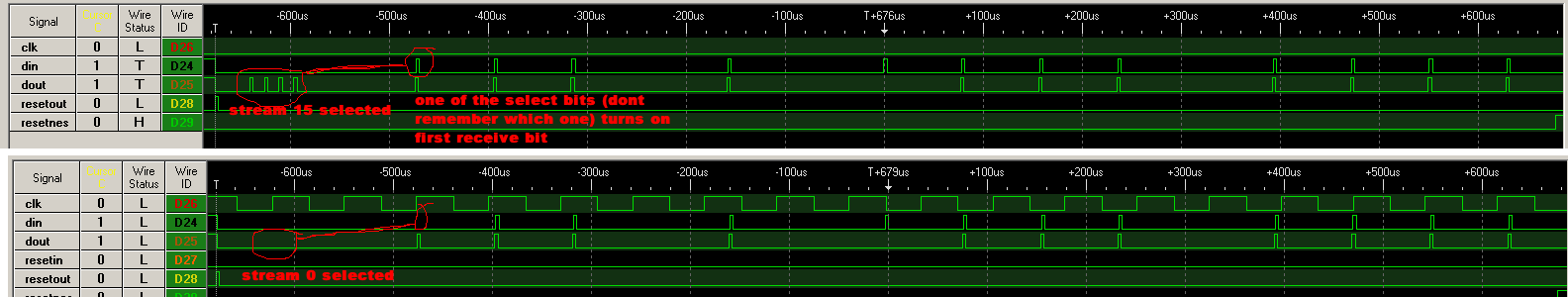
Just to make this post even longer, here is a bit more information about the initial transaction. One of the bits in the stream select triggers the first bit received from the cart. I dont remember which stream bit it was tho... Here is a picture with some stuff circled. All other bits are always the same until the reset line goes high. Once again ignore the clock in the picture.
On the pictures: a line up means 5 volts, logic 1. Line down means 0 volts, logic 0. The numbers at the top (-600uS, 300uS, etc) are the time scale, relative to the center of the screen. We dont know how fast the bit rate is, so 600uS != 600 bits. Any number with a T in it (T, T+676uS, T+2.8mS, etc) is relative to the trigger, which in this case is the beginning of the sync pulse. This shows in the second transaction picture that everything is happening ~2.5mS after the sync pulse.
The bit transfers are slightly shifted, with the nes cic sending before the cart cic sends. You can see them shifted 1-2 pixels which is probably 1-2 clock cycles. Most likely the nes cic sends then receives, the cart cic receives then sends
The logic analyzer runs at up to 500MHz, I usually use 100MHz which very easily captures everything accurately. The pictures are just screenshots so its not easy to get long sequences. I can also save state transition tables but I do not know of a good program to view those. It would help lots, anyone know of one? Sample state transition table: 10nes.csv
Just to make this post even longer, here is a bit more information about the initial transaction. One of the bits in the stream select triggers the first bit received from the cart. I dont remember which stream bit it was tho... Here is a picture with some stuff circled. All other bits are always the same until the reset line goes high. Once again ignore the clock in the picture.
bunnyboy wrote:
We also dont know if the bits represent values. The protocol could be running a timer and counting the clocks between high bits.
What is the distribution of clocks between high bits? If someone could make a histogram out of the CSV file, that would be nice. Then we could tell if it's counting the clocks (for example: generate number, wait that many cycles, output 1, output 0) or if it's comparing (for example: generate number, if equal to 0 output 1 else output 0). If the time between 1's is roughly uniformly distributed, it's generating and waiting; if it's non-uniform, it's generating constantly and comparing.
Quote:
The logic analyzer runs at up to 500MHz, I usually use 100MHz which very easily captures everything accurately.
Could you go down to 32 MHz or 16 MHz for some captures so that you can get more data at once while still appreciably oversampling to remove aliasing artifacts? Does your analyzer support synchronizing to a multiple of the CIC clock, or must it always run asynchronously?
tepples wrote:
What is the distribution of clocks between high bits? If someone could make a histogram out of the CSV file, that would be nice. Then we could tell if it's counting the clocks (for example: generate number, wait that many cycles, output 1, output 0) or if it's comparing (for example: generate number, if equal to 0 output 1 else output 0). If the time between 1's is roughly uniformly distributed, it's generating and waiting; if it's non-uniform, it's generating constantly and comparing.
I think it will be a bit harder than that because of the apparent chunks of important data. It looks like there is a big pause then a set of 1/0s then another big pause. I will have to capture more data....
tepples wrote:
Could you go down to 32 MHz or 16 MHz for some captures so that you can get more data at once while still appreciably oversampling to remove aliasing artifacts? Does your analyzer support synchronizing to a multiple of the CIC clock, or must it always run asynchronously?
When I run the analyzer fast I have compression which means only state transitions are stored. Number of transitions is the limit, not time (which is why I dont capture the clock signal). I havent played with other modes but I should be able to capture everything for long periods of time. The parallel port to control clock signal would probably be better at that tho.
I can do synchronous but only on transitions of one direction and I think important stuff happens on rising and falling edges of the clock.
I really want to get theese things hooked up to a Parallel port. I'll try to do it this weekend. Anybody prefer I store the data a certian way?
I was thinking of just making a list of numbers the first number is how many clock cycles low, then keep alternating back and forth. This would greatly reduce the file size and I would think be pretty easy to analize. It would look like this: 1,2,4,1 would represent LHHLLLLH. L and H being low and high respectively.
I like bunnyboys approach to how this thing works. I was thinking it probably counts the clock cycles to hold Dout low too. Also perhaps the meaningfull data is simply the next random number. It could alternate between using the random number to output clock cycles and then it takes the next random number and just sends it's value serially. Just a guess though.
If it does generate random numbers then it's possible the Lock sends the seed as it's method of stream selection. I hope this is the case, cause then we can simulate a lock chip and send it different seeds. Sending all zeros for a seed would show us if any of the bits are ORed or XORed. All ones could reveal possible AND and XOR instructions. If anyone's intrested in using the parallel port to gather info, but doesn't have the low level digital electronics knowledge to set it up let me know and I will post my schematics and the source code too, as soon as I get it working good.
Zack S wrote:
If it does generate random numbers then it's possible the Lock sends the seed as it's method of stream selection. I hope this is the case, cause then we can simulate a lock chip and send it different seeds. Sending all zeros for a seed would show us if any of the bits are ORed or XORed.
Yeah right. I'd bet it looks up the seed in a table.
tepples wrote:
Yeah right. I'd bet it looks up the seed in a table.
You shot that idea down pretty quick. I bet you're right though. None the less I'll still check.
Quote:
I was thinking of just making a list of numbers the first number is how many clock cycles low, then keep alternating back and forth. This would greatly reduce the file size and I would think be pretty easy to analize. It would look like this: 1,2,4,1 would represent LHHLLLLH. L and H
Use something that isn't so fragile. How about the format of the logs posted, where they are composed of state snapshots with the delays between them?
As for the algorithm, it could be quite complex and not at all simple to understand. As long as it's deterministic, they could just throw random code together with some design. They were smart to have the devices share very little data. What might help is to systematically reason about things the chips must be doing, and things they can't be doing. That will clearly outline the limits of theories.
They can be doing DES, where a chip can generate one of 32 DES keystreams (16 for lock and 16 for key) and verify the other one.
.
kevtris wrote:
This is the length distribution graph that Q made:
http://tripoint.org/kevtris/mappers/inc ... bution.jpg
http://tripoint.org/kevtris/mappers/inc ... bution.jpg
Fuck me?
(You forgot to add nesdev.com and nesdev.com to the whitelist.)
.
I tried to get my parallel port to log the CIC in action but had no luck. Not sure what the problem is. I'm sure I'll get it right eventually. Or maybe I'll just do what Kevin suggested and break out a FPGA.
While messing with the CIC logger I was trying to make, I got an idea on another way to beat this system. When no cart is in the NES, the system isn't in reset the whole time. If we could disrupt the clock signal going to the Lock while the system is on, the lock won't be able to function and the NES will stay on. Ofcourse for this to work it would require messing the clock signal up enough to halt the MPU in the lock. But at the same time it can't damage the oscillator. Would this be possible?
I got it to work on the bread board pretty easily by just removing the clock signal wire. Anybody know a good way to stop the clock without damage? I have no problem with testing this on one of my nintendos, worst case scenario I have to remove the CIC altogether.
You could always open a Game Pak, cut pin 4 on the CIC, and then wire up two Game Paks' CICs in a lock/key configuration.
tepples wrote:
You could always open a Game Pak, cut pin 4 on the CIC, and then wire up two Game Paks' CICs in a lock/key configuration.
I think you'll need to wire the pin to VCC, not just cut it. Cut it on the NES PCB has the effect to tie it to GND, for some reason. But it won't be the same between 2 game paqs. And yeah, that is a great idea, because there is no NES invoved, and this avoid lots of problems, such as risk to damage the console or mecanical issues.
Bregalad wrote:
tepples wrote:
You could always open a Game Pak, cut pin 4 on the CIC, and then wire up two Game Paks' CICs in a lock/key configuration.
I think you'll need to wire the pin to VCC, not just cut it.
I intended that to be implicit in "wire up two CICs in lock/key". You cut pin 4 so that you can turn a key into a lock. Or you can just desolder the two CICs completely and put them in a breadboard.
Quote:
And yeah, that is a great idea
Thanks.
Has anybody tried to photograph the insides of the Rabbit chip from Tengen games yet?
tepples wrote:
I intended that to be implicit in "wire up two CICs in lock/key". You cut pin 4 so that you can turn a key into a lock. Or you can just desolder the two CICs completely and put them in a breadboard.
Disolver a 14 pin DIL chip on a PCB with solver on both sides without doing serious damage to the chip is nearly impossible.
Assuming "disolver" is supposed to be "desolder", you're wrong - you can most certainly desolder a 14-pin DIL chip from a double-sided board without damaging it IF you have the proper tools. With a decent desoldering iron, it's quite easy, though it's still doable with a spring-loaded solder-sucker (but slow) or even copper braid solder wick (though it'd take a LONG time).
Zack S wrote:
I tried to get my parallel port to log the CIC in action but had no luck. Not sure what the problem is. I'm sure I'll get it right eventually. Or maybe I'll just do what Kevin suggested and break out a FPGA.
The problem is, you must reset the CIC for it to start working. If you don't, the CIC will get very hot! I dunno why this is, but it does. When working normally, the CIC does not get warm.
Quote:
While messing with the CIC logger I was trying to make, I got an idea on another way to beat this system. When no cart is in the NES, the system isn't in reset the whole time. If we could disrupt the clock signal going to the Lock while the system is on, the lock won't be able to function and the NES will stay on. Ofcourse for this to work it would require messing the clock signal up enough to halt the MPU in the lock. But at the same time it can't damage the oscillator. Would this be possible?
That won't work. They use two separate inverters on the 74HCU04 to individually buffer CLK to each CIC.
Quote:
I got it to work on the bread board pretty easily by just removing the clock signal wire. Anybody know a good way to stop the clock without damage? I have no problem with testing this on one of my nintendos, worst case scenario I have to remove the CIC altogether.
Just remove two CICs from two cartridges and use those... Though I am unclear if you can use the 6113 CICs back to back.
Speaking of this, I am kinda confused about why nintendo did this. The console *always* has a 3193 CIC in it (US console), while the carts have a 3193 (older) or 6113 (newer). I was wondering if the 6113 was a "key only" cost-reduced version or something... Even the very last versions of the front loader have the 3193 in it... So there must be some reason the 6113 is not usable as a lock.
kevtris wrote:
The problem is, you must reset the CIC for it to start working. If you don't, the CIC will get very hot! I dunno why this is, but it does. When working normally, the CIC does not get warm.
I had a Reset signal going to the Lock and a Clock signal going to both CIC's. It's probably just something wrong with my code or I misswired something.
kevtris wrote:
That won't work. They use two separate inverters on the 74HCU04 to individually buffer CLK to each CIC.
Guess it's back to trying to RE it.
kevtris wrote:
Just remove two CICs from two cartridges and use those... Though I am unclear if you can use the 6113 CICs back to back.
That's excactlt what I did. Both of the CIC's are 6113's that I took out of game carts. They work fine back to back, at least they seem to. Without the key connected it produce the reset squarewave for the NES. With the key connected it kept the NES out of reset.
Bredalad wrote:
Disolver a 14 pin DIL chip on a PCB with solver on both sides without doing serious damage to the chip is nearly impossible.
I used a 15$ desoldering iron to pull two CIC's off of PCB's, it took about a minute each. They worked fine in the breadboard so it didn't damage them. I usually do every 3rd pin or so, as opposed to just going down the line. That way each area of the chip has time to cool.
has anyone logged what the lock and key do when they are not connected to each other? also... has anyone logged the response from the key when given only part of the sequence from the lock and vice versa?
The legal docs from the Nintendo vs Tengen case mentioned that Nintendo modified the lockout code in 1987 ("deleted some instructions"), maybe that's when they changed the part #s for the chip?
WhoaMan wrote:
has anyone logged what the lock and key do when they are not connected to each other? also... has anyone logged the response from the key when given only part of the sequence from the lock and vice versa?
I haven't yet but plan to as soon as I get my data logger working. I got an oscilliscope toady so that should help me figure out whats not working.
Zack S wrote:
I got an oscilliscope toady so that should help me figure out whats not working.

Oscilloscope toadies from Yoshi's Island 2: Reverse Engineering
Quick update on my Parallel port data logger project. This will simply not work. I hooked up the O-scope and found that the parallel port can't go fast enough for the CIC. I'm guessing that the part of the chip depends on dynamic RAM, that isn't getting refreshed fast enough with the slow clock cycle I'm giving it.
I'm still learning to work with FPGA's so it could be some time before I make a data logger for it.
I'm still learning to work with FPGA's so it could be some time before I make a data logger for it.
I really doubt it has dynamic RAM in it. It could be some other asynchronous element in it like the older time-delay digital logic design that uses resistors and capacitor (RC) elements instead of clocked logic.
Moved from NESdev to NES Hardware / CopyNES, as the CIC's functionality isn't really related to NES programming.
kevtris wrote:
One interesting thing is that there are no runs shorter than 87 clocks I believe it was. In all my testing, one "clock" was made up of 4 clock cycles to the lockout chips.
I was thinking about this, comparing it to the patent document, and it doesn't make sense to me. According to the document there is the initial exchange, to seed the first random number (select the sequence) and then there is a transaction once per 4 clocks. I'll explain:
The 4Mhz clock is divided by 4 and split into four separate clocks in each of the four possible phases - and they are called phi1 through phi4. The patent suggests that on phi1 data is read in from the IO port. The next two cycles (phi2 and phi3) are used for "predetermined arithmetic operations". Then, on phi4 the data is output to IO. This sequence is repeated indefinately.
If I'm understanding this correctly, the data that is read in on phi1 as well as the data output in phi4 can't be anything other than 1 bit in size. It seems unlikely that the distribution would allow for runs of 87 cycles and longer without a single result of "1". Am I missing something here? Are the patent documents not quite accurate? I'm very suspicious of the explaination of the synchronization explained in there, it doesn't match the logic analyzer logs posted.
edit: I just realized that the "1" in the logs from Kev's tester are 3 clocks long.... which is a big clue. It indicates it's operating on the divided clocks and not on the original. I'm thinking there's some kind of "pipeline" going on here.
bunnyboy wrote:
I put all my text files in a new directory at www.nesmuseum.com/10nes
nescicrom.txt - nes lockout rom dump, directly from rom array. Bits and bytes are interleaved, figuring out how it is actually arranged is part of the problem.
nescicrom.txt - nes lockout rom dump, directly from rom array. Bits and bytes are interleaved, figuring out how it is actually arranged is part of the problem.
I had downloaded the photos taken by Nevitski with the microscope of the NES CIC, and started to decode them myself. I didn't make it all the way through - only 144 bytes in. However, comparing what I have against what you posted I found a discrepancy. Below I will paste the content of your nescicrom.txt, but will put an "X" in the location where I came up with a different value than you did. You have a "1" in that spot, and I read it as "0". In the 1152 bits that I decoded, we only differ by one bit... which means we're either reading it correctly, or at least consistantly incorrect.
1111100010111010001110100111111001111110010111000011101011101110
0110011110111111001101011111X11101100101011011010011010111011111
Unfortunately one bit difference out of over 1000 doesn't help us decode it at all. But it points out having several people decode it independently might help us reduce errors in it. If I get time, I'll try to keep decoding more.
Contrary to what a lot of people think, Motorola DID design a 4-bit cpu:
The MC141000.
This MIGHT be the processor used in the Tengen CIC clone.
I managed to dig up the datasheets for it in one of the lab rooms around campus, where they had copies of many of the old Motorola databooks.
As far as I'm aware, the datasheets are unavailable on the internet.
The last page has the instruction set on it.
Scans: (note that these require some image rotation)
http://www.netaxs.com/~gevaryah/MC141xxx001.png
http://www.netaxs.com/~gevaryah/MC141xxx002.png
http://www.netaxs.com/~gevaryah/MC141xxx003.png
http://www.netaxs.com/~gevaryah/MC141xxx004.png
http://www.netaxs.com/~gevaryah/MC141xxx005.png
Lord Nightmare AKA Jonathan Gevaryahu
lord(underscore)nightmare (@t) users (d0t) sf (d0t) net
Lord Nightmare wrote:
Contrary to what a lot of people think, Motorola DID design a 4-bit cpu:
The MC141000.
This MIGHT be the processor used in the Tengen CIC clone.
The MC141000.
This MIGHT be the processor used in the Tengen CIC clone.
How surprising, I've never heard of it. The only 4-bit CPU I've ever heard about it the Intel 4040.
Might it be the processor used in the real CIC microcontroller ?
Kevin since you already have a data logger on hand. Maybe you could program it so instead of just recording the whole stream of data, It could record the first few transitions and then just keep looking for it to repeat. Then we might be able to find out how long it takes to repeat with out having to fill up a harddrive. That could give us a pretty good idea of how secure it really is.
Zack S wrote:
Kevin since you already have a data logger on hand. Maybe you could program it so instead of just recording the whole stream of data, It could record the first few transitions and then just keep looking for it to repeat. Then we might be able to find out how long it takes to repeat with out having to fill up a harddrive. That could give us a pretty good idea of how secure it really is.
It's not possible to "look for it to repeat" without logging the entire data stream. The last stream kevtris logged was nearly 7 minutes worth of real-time data - which took many hours to dump and occupied over 400 megabytes of space (since it stored only 1 cycle per byte, using a few of the upper bits for sequence numbers to make sure the serial datastream never skipped any bytes) - and it didn't repeat.
Quietust wrote:
It's not possible to "look for it to repeat" without logging the entire data stream.
I don't understand why you come to this conclusion. You record a very short sample of the stream when it begins, then simply read the stream following and if it doesn't match the recorded beginning discard the data and retrieve the next section. Since the signal is so sparse it should allow plenty of time for the comparison. Once you find a spot that matches you could verify that it is repeating by restarting and logging every Nth number output that way you don't need huge amounts of data but still get a good comparison to verify it is indeed repeating.
On another topic. I have read the cherryrom forum like 3 times now and gone though the patent twice. How feasable would it be to try and read some of the CPU core circuitry. I have a pretty good knowledge of this sort of thing and could probably produce most of the instruction set if I had a good schematic of the CPU Core. I would be willing to get a microscope and other needed items if It would allow me a better look at the internal circuitry.
Has anyone already taken usable pictures of this already?
Thanks again for all the help.
Considering how random the data is, you would have to read a very long segment in order to insure that the data really DID repeat - otherwise you could easily be thrown off. Consider this example:
123456789079084325897324059734850972348509724509872435809723450987908790837980790825902835
123456789013459632485732459534759018709463298174893274980632174612409382754326574359083745
123456789078346159045967094586767096867860983568920359034868798089748679827349580734985737
Using your logic, you would have detected two repeats based on the string "1234567890", but the string clearly does not repeat at all in the sample space provided.
Why is everyone expecting the stream to repeat? Maybe it just wont. I don't know much about this, and I should probably be quiet, but I think that decoding the program is still the best bet.
It really amazes me that this thing wasn't figured out yet... This chip is so old and there are so many amazing people in nesdev! it is a mistery why this chip wasn't figured out yet.
It really amazes me that this thing wasn't figured out yet... This chip is so old and there are so many amazing people in nesdev! it is a mistery why this chip wasn't figured out yet.
Quote:
It really amazes me that this thing wasn't figured out yet... This chip is so old and there are so many amazing people in nesdev! it is a mistery why this chip wasn't figured out yet.
I agree, plus all SNES dev people have the same sheme.
All random number generation repeats, even if the string is very very very long. However, since the binary has been decoded, I think, some people that are able to do it should try to see what it looks with all processors back then.
Quote:
Why is everyone expecting the stream to repeat? Maybe it just wont. I don't know much about this, and I should probably be quiet, but I think that decoding the program is still the best bet.
The two chips both generate a sequence and verify that the other is generating the same. Unless they somehow connect to a single quantum random number source or something (only joking here), the sequence must be generated using a finite deterministic process, thus it must repeat. Repeatability is the same principle that lets emulators record movies by only keeping the joypad input.
Bregalad wrote:
However, since the binary has been decoded, I think, some people that are able to do it should try to see what it looks with all processors back then.
I have been trying to work with the ROM dump, but everyone seems unsure of how it is interleaved, where the data bus connects, how the address is decoded etc. A lot of the HEX code generated, has been either 0 or F wich doesn't seem right to me. Unless they're no op instruction inserted in the code for timing purposes.
Not to mention some other unknowns like how the key/lock pin is connected. It could be a port that is read or it could simply be hooked up to the ROM's highest address bit, effectively dividing the ROM into two seperate chunks. One for each function.
If we knew for sure that we are looking at the instructions in sequential order, I'm sure we could attach some meaningfull assembly commands to the code using the 10NES flow chart.
Well, I really cannot say anything here, because I really have no experience with reverse-engineering.
May I ask a stupid question ? How was people able to reverse-engineer the NES (or other machines) to figure out how the PPU, APU cartridge banking, etc... works ? Okay, it is said that the console have a 6502 and you can read the text inside the cartridge to know wich chips are the maskrom, but you don't know their pinout, and you don't know wich bus adress is what, etc...
It seems just impossible to figure out. Well, the very first older NROM game has regular pinout, so it would be possible to dump them, and to look at the 6502 code to figure out how the registers are written to. From there, you can replace the ROM, and try about anything. So you can figure pretty much how the adress buses works, and so can work with more advanced cartridge. However, with absolutely no known about how works pattern tables, name tables, palettes, it would be long long hours of work to try to change any value from the original game to see what's happening.
That's for NES, but for SNES, the hardware is much more complicated. And for the GBA, due to the size of the cartridges, the fact that everything is surface-mounted, etc...... well, I stop saying stupid things. Those HAD been reverse-engineered.
The simple answer to why this hasn't been reverse engineered is that it's really difficult. It's much more difficult than an MMC chip for example, because it's external interface doesn't give away much of what it does. If you want to get an idea of how difficult it is, read this phd thesis on the topic:
Intro
http://www.cl.cam.ac.uk/~sps32/mcu_lock.html
Full paper
http://www.cl.cam.ac.uk/TechReports/UCAM-CL-TR-630.pdf
There are several interesting and pretty doable approaches mentioned there, but the equipment and cost for most of them is pretty steep. Our best bet is to get a full optical picture of the decapped chip, learn some VLSI, and start RE'ing the thing. The full optical scan is very difficult unless you have a microscope that does this automatically, because at the 500x magnification you need, you need to take a LOT of photos and stitch them together.
Although, if we can decode enough of the area around the ROM to learn how the bits are interleaved, that's a pretty good start.
Bregalad wrote:
Well, the very first older NROM game has regular pinout
I once read a story of how an unlicensed shop (Color Dreams? Tengen?) cracked the NES. At that point, they had dumped the PRG ROM and CHR ROM of Mario Bros. PRG was found to contain byte sequences common in 6502 bytecode, and CHR was decoded using a simple tile editor similar to those used to develop for other consoles, 8-bit microcomputers, and arcade systems. With the CHR, they could discover the character encoding that the PRG uses for text.
Bregalad wrote:
However, with absolutely no known about how works pattern tables, name tables, palettes, it would be long long hours of work to try to change any value from the original game to see what's happening.
A bit/bpl loop means "wait for this bit to become set", so $2002 must be a status register of sorts that periodically sets bit 7 to 1. This is enough to get the game into an infinite jmp loop when running in a generic 6502 simulator. An infinite loop likely means that the program is waiting for an interrupt to do something, so they explored the vectors and saw what happened when they triggered NMI.
At the same time, they searched for text in the ROM and then pointers to that text. A write-to-screen subroutine would use such a pointer to text. In the generic 6502 sim, place a breakpoint on reads from addresses inside text strings, and the PC is likely to be within a write-to-screen loop. So $2007 must be an output port to which things are written. Et cetera.
But if you don't have access to the PRG ROM bytes in order, and/or the processor's architecture is unfamiliar, you can't do all this as easily. Heck, unlike with carts soldered onto a PCB, you don't even have any traces to plug in a logic analyzer.
You mean reverse engineering is usually based by seeing how the silicium connexions are made inside the chip ? That's real crazy. It would take an incredible number of days to fully understand what those little connexions mean. Well, I think this is usefull anyway, even if it is a lot of hard-work.
I just got a pile of World Class Service tech manuals, there is sooo much interesting stuff in them. There is almost no information about the CIC but some of the cart pinouts have a more detailed pinout of the CIC. No idea how this helps anything...
1 OUT (to nes)
2 IN (from nes)
3 R02 (unconnected)
4 SEL (gnd, lock/key)
5 CL2 (unconnected)
6 CLK (from nes)
7 RST (from nes)
8 GND
9 R10 (unconnected)
10 R11 (unconnected)
11 R12 (unconnected)
12 R13 (unconnected)
13 R20 (unconnected)
14 R21 (unconnected)
15 R22 (unconnected)
16 Vcc
Some of the other cart schematics show R02, R12, R13, R20, R21, R22 connected to ground, but R10, R11, CL2 still unconnected.
we should try dumping the 16 streams that the lock spits out from when it is first powered until it toggles the 1hz reset line... then compare these to the 16 streams spit out by both the Lock and Key and try to determine where the break in communication affects the lock. has anyone logged the streams in an unconnected CIC?
So how's the electron microscope effort coming along?
-Rob
-Rob
Speculation based on loopy's data: the nes CIC patent is correct: the clock is divided by four before it is used by the chip internals.
according to the patent:
phase 1(0) = cpu reads input
phase 2(1) = arithmetic operation 1
phase 3(2) = arithmetic operation 2 or continuation of 1
phase 4(3) = cpu sets output (external lines come active on the ?falling edge of this clock? according to column 5, line 35-40 in the patent)
my guess for the first cycle of the cic based on the patent is it reads pin 5 and does a conditional jump (or less likely, a variable set) depending on whether it is a lock or key. I can't tell much else.
Also the preamble transmitted by the master? cic seems to be for both key specification (i.e. master provides TWO 4-bit numbers to the slave, one is 'my key' and one is 'your key', hence how both know which key the other is sending to compare to) and to phase-desynchronize the slave cic to it somehow, because if both chips were running at exactly the same phase, the patterns of ..0001332000.. we see wouldn't show up, they'd be ..000333000..
Lord Nightmare AKA Jonathan Gevaryahu
lord_nightmare (@t) users (d0t) sf (d0t) net
If someone wanted to post a binary or text version of the CIC output and provide hours of data I would want to number crunch it. I think saving the timestamp and states when the state does change would be a good format. I don't mind trying to brute force this thing but if we're going to do it that way I will need lots of data to analyze.
I do appreciate the data already posted but I'll need more to try to brute force this thing. I don't have the neccessary equipment to record the pulses or I would be working on this on my own.
I do appreciate the data already posted but I'll need more to try to brute force this thing. I don't have the neccessary equipment to record the pulses or I would be working on this on my own.
I think there's only one 4-bit key. It may be that the key generates pairs of pseudo-random bits at a time, with the lock sending one of the two bits and the key sending the other.
I doubt that the misalignment between the two CICs (the "013320") has any significance. It's probably just a side-effect of how the chips get synchronized (one happens to be one step off). My guess is the CIC follows a procedure like "Write output; Read input; Wait a cycle; Clear output"), where the setting and clearing of the output data occur three steps apart and the reading occurs in the middle. As long as the middle read occurs while the other chip still has valid output, the system will work even if the chips are slightly out of alignment (which is obviously the case).
I doubt that the misalignment between the two CICs (the "013320") has any significance. It's probably just a side-effect of how the chips get synchronized (one happens to be one step off). My guess is the CIC follows a procedure like "Write output; Read input; Wait a cycle; Clear output"), where the setting and clearing of the output data occur three steps apart and the reading occurs in the middle. As long as the middle read occurs while the other chip still has valid output, the system will work even if the chips are slightly out of alignment (which is obviously the case).
This topic has interested me for a couple of year.
It would be very interesting to know how the CIC works.
A very good start would probably be to dig out all information on
4 bit micros around that time and then write dissassemblers for them.
Assuming the bitordering is done correctly it would probably
show right away, as long as it's not a custom type cpu.
If the instructions makes any sense it's probably a candidate cpu.
It could be as the maincpu of the gameboy, a standard cpu (in this case z80) but modified to a certain degree.
I tried to look up some datasheets of old 4 bit micros, but it's really a jungle.
That im limited to a 56k modem at the moment doesn't really help either -_-
One way might be to try to find docs of who were nintendo partners at
the time, possibly numbers. As CICs were included in about every game,
it would probably showup somewhere.
Hello,
Sorry for the long pause. Cherryroms is down, so I guess I'll continue this here. (Grrr... I'd like to be able to see my old posts/thoughts/work)
http://www.neviksti.com/CIC/tengen/
as the name suggests, this is the tengen CIC. I believe this is currently our only real hope of figuring out the program. The first thing is to identify the core used here (it is indeed something from Motorola, and appears to be 4-bit according to the SRAM organization). So have at it!
I have access to a much better camera now (for those that remember what the other CIC pictures looked like). I love the old chips, it is so easy to see everything! These pictures were taken with only a 100x lense. The next one is 500x, and I wasn't willing to take 25 times as many pictures as this alone took me two hours, so this is it for resolution. You can make out almost everything, so I think it will be okay for those that wanted to "trace" the circuit.
Reminder, there are three layers here: (top to bottom) metal, poly-silicon, bulk/silicon surface (you can sometimes make out the edges of the different doping regions).
I'm tired and think I'm done for the night. Can someone please combine these into a nice "one large picture", and maybe a shunken/overview version of that as well? It would be quite helpful.
I took the pictures snaking my way down the chip (ie every picture is adjacent to the last one), like this:
If you put the pictures together, you can upload it to a ftp space I setup here for everyone:
ftp.neviksti.com
user: CICpub
pass: pub987A
I'd also like to get all the CIC information people have into one place, so please ... if you have anything you think may be useful, please upload it for everyone to be able to read. Now that I have a bit more time, hopefully we can work together and figure out the mystery of this chip.
-neviksti
Sorry for the long pause. Cherryroms is down, so I guess I'll continue this here. (Grrr... I'd like to be able to see my old posts/thoughts/work)
http://www.neviksti.com/CIC/tengen/
as the name suggests, this is the tengen CIC. I believe this is currently our only real hope of figuring out the program. The first thing is to identify the core used here (it is indeed something from Motorola, and appears to be 4-bit according to the SRAM organization). So have at it!
I have access to a much better camera now (for those that remember what the other CIC pictures looked like). I love the old chips, it is so easy to see everything! These pictures were taken with only a 100x lense. The next one is 500x, and I wasn't willing to take 25 times as many pictures as this alone took me two hours, so this is it for resolution. You can make out almost everything, so I think it will be okay for those that wanted to "trace" the circuit.
Reminder, there are three layers here: (top to bottom) metal, poly-silicon, bulk/silicon surface (you can sometimes make out the edges of the different doping regions).
I'm tired and think I'm done for the night. Can someone please combine these into a nice "one large picture", and maybe a shunken/overview version of that as well? It would be quite helpful.
I took the pictures snaking my way down the chip (ie every picture is adjacent to the last one), like this:
Code:
--------+
|
+-------+
|
+-------+
|
+-------+
|
... etc
|
+-------+
|
+-------+
|
+-------+
|
... etc
If you put the pictures together, you can upload it to a ftp space I setup here for everyone:
ftp.neviksti.com
user: CICpub
pass: pub987A
I'd also like to get all the CIC information people have into one place, so please ... if you have anything you think may be useful, please upload it for everyone to be able to read. Now that I have a bit more time, hopefully we can work together and figure out the mystery of this chip.
-neviksti
Oh, I almost forgot...
I also depackaged a 6113A and 6113B1 (from US cartridges). I didn't take time to look at them under the microscope yet, but the B1 is smaller than the A. So it is probably just the same exact circuit and code, just taking advantage of newer fabrication technology.
And one last thing, I can see details much better than the camera made out, so I will hold off on trying to read the ROM in case people need to see a small portion better (because I have to etch away all the upper layers to get at the ROM ... in other words, if you have questions, ask them now as there is no looking back). I won't have time to try reading the ROM for awhile anyway, and if people want me to hold off even longer, of course that is fine as well.
Thanks. It's like christmas. But with a harder to open package.
Just shooing from the hip here (like I always do):
Is it completely out of the question to attempt to emulate the chip's actual function based entirely on the physical model of the chip? I mean, if all the transistor junctions are visible, then it's technically as good as a *really* hard to read schematic, right?
Of course the hard part would be automating the translation of that image data, as I'd imagine that doing it by hand would be far to error-prone. It would take some juggling of the contrast of each layer to bring out the right features, and then applying some image analysis.
I wouldn't expect to get a 100% perfect emulation out of such a thing. Instead, maybe something that can at least behave like a state machine, so the inner-workings of this thing can become a little more scutable. I'd suspect that things like on-chip inductors, capacitors, transistor switch timings (and god only knows what else - I'm no EE) would keep a few things out of reach, but the rest is doable IMO.
Glad to see you are back! The cherryroms forums are still in google cache, go grab them quick while you can. Let me know if you need me to send you more cic chips in case the first ones dont work.
The ASIC in picture 4 isnt promising, but it could just mean its standard micro inside custom package. I think the assumption has always been it was an 8 bit cpu because of the link to motorola. Mapping out every transistor will be crazy time consuming but could be the best option. I cant recognize transistor/gate structures, anyone have links to tutorials?
The ASIC in picture 4 isnt promising, but it could just mean its standard micro inside custom package. I think the assumption has always been it was an 8 bit cpu because of the link to motorola. Mapping out every transistor will be crazy time consuming but could be the best option. I cant recognize transistor/gate structures, anyone have links to tutorials?
WOW...awesome. Just how many layers are there?
-Rob
-Rob
pragma wrote:
Just shooing from the hip here (like I always do):
Is it completely out of the question to attempt to emulate the chip's actual function based entirely on the physical model of the chip? I mean, if all the transistor junctions are visible, then it's technically as good as a *really* hard to read schematic, right?
Is it completely out of the question to attempt to emulate the chip's actual function based entirely on the physical model of the chip? I mean, if all the transistor junctions are visible, then it's technically as good as a *really* hard to read schematic, right?
I had the same idea at one point. It seems possible to extract the netlist from the photo's, and create a model of the hardware using SPICE. Then, we could have a dynamic model to play with to help with the reverse engineering, as opposed to just the pictures.
I came to the conclusion that while feasible, it's a lot of work. I would consider it as a last resort, but I don't see it as impossible.
BTW, thanks a million Nevitski, your effort is much appreciated.
rbudrick wrote:
WOW...awesome. Just how many layers are there?
-Rob
I tried to answer this in my earlier post:
-Rob
Reminder, there are three layers here: (top to bottom) metal, poly-silicon, bulk/silicon surface (you can sometimes make out the edges of the different doping regions).
If you just overlooked it, that's fine, but if you are referring to something else and I'm misunderstanding, just let me know and I'll try to answer the question.
As for "complete specification" of the circuit ... nope, these pictures will not allow you to know all of that. Even though there are only three layers, the upper ones cover too much to completely see the lower ones. In particular, it is amazing that any of the diffusion layer can be seen.
What can these pictures be used for?
- You can see the organization of the memory (I still can't tell how many bits are in one instruction, can someone tell?).
- You can see how the address lines connect.
- You may be able to identify other components and how they connect / interact (to help determine the CPU core).
- An industrious individual may even be able to identify how the opcodes are "grouped" (ie usually all move commands have a vary similar opcode ... you could think of it as a couple bits are the "command" and other bits are the "arguements").
- Hopefully someone can figure out how the ROM bits are ordered before we try to read them out.
If you guys really want, I can try to remove just the upper oxide and metal interconnect layer, to get pictures of the middle layer. Then you probably could trace the entire circuit. I'm not confident I can remove the layers like that though.
As far as ASIC goes, I don't expect much to be custom besides the location and handling of the power and I/O pins. It would be wasteful of resources for them to try to create their own CPU core.
I seem to remember reading that the Tengen CIC clone was based on a standard Motorola 6800 series core.
tepples wrote:
I seem to remember reading that the Tengen CIC clone was based on a standard Motorola 6800 series core.
Where did you read this? I would like to check up on it if you have a lead.
Also, as usual, it is always worth it to pursue this from the human angle. Check out this article:
http://www.atarihq.com/tsr/special/el/el.html
Ed Logg: I walked into the lab and they were reverse engineering the chip, and I asked what they were doing and they said "Don't ask". (laughs) So I know the company was doing it, and I knew the people involved doing it.
It is a starting lead. All we need is for them to tell us what CPU core they used (I think this is a reasonable/possible question to get an answer to). Anyone willing to follow the trail?
Wow, killer interview. I'm surprised I hadn't seen that before.
Neviksti, if you are reasonably sure there's a good chance you can get to the other layer, I say go for it. It would probably be pretty useful.
Did anyone stitch these scans together?
Would it be easier to get the other side if you got another chip and went in through the bottom instead? Just a shot in the dark here since I've never pulled a chip like this apart before.
-Rob
Yeah, there's a stitched together pic on the server.
I wish I could tell more about it just from looking at the pics. I can't find any reasonably hires pics of many Motorla chips, from the looks of it I was lucky to find a pic at all of the 6800 here:
http://www.cpu-world.com/CPUs/6800/die/L_Motorola-MC6800L.jpg
http://www.cpu-world.com/CPUs/6800/die/L_AMI-S6800.jpg
rbudrick wrote:
Neviksti, if you are reasonably sure there's a good chance you can get to the other layer, I say go for it. It would probably be pretty useful.
I thought about it and decided I'd like to make sure we're "done" with this top layer first, before continuing.
(I'm willing to take higher res photos of small regions, like how the SRAM is addressed, and how the ROM is addressed or something. However, due to the time required, I probably won't do that unless there's a specific thing I'm looking for... specific connection question I am trying to answer that can't be seen in the current pics.)
rbudrick wrote:
Would it be easier to get the other side if you got another chip and went in through the bottom instead? Just a shot in the dark here since I've never pulled a chip like this apart before.
It isn't feasible to come in from the back side of the chip.
Of the three layers, the top and bottom are easy to get at. The top for obvious reasons, and the bottom because it is just the silicon surface ... so I can etch everything above it away with HF and/or Nitric acid, without any worry of hurting the bottom layer. It is the middle layers that are difficult to get at (I "kind of" did it successfully once for a chip that had a security / copper mesh layer on top, but it wasn't all that great.).
---------------------
To get more focussed:
We need to start with reasonable/simple questions first. Such as:
1] How much SRAM is there? How is it organized (4-bit? 8-bit?)
2] How much ROM is there? How is it organized (8-bit? something else?)
3] Do the ROM / SRAM share a common data bus and address bus?
These are feasible questions.
Since we already know the manufacturer, this greatly narrows our search.
I'm not all that confident in my answers to some of these questions, and so would really like confirmation.
If you're not sure where to start, first read up on what an FET is - as all CMOS circuitry is built up from these transistors. Important to note is what this would look like in the picture:
- the top layer (the metal) is used to relay signals around the chip
- the middle layer (the polysilicon) is used as the gate signals for FET's (note: one long line of polysilicon can be controlling many transistors) or just to move signals under the metal layer (kind of like a two layer circuit board)
- the bottom layer (the diffusion layer / bulk silicon surface) can't be seen much in the pictures, and doesn't usually matter for these level of questions (but without this, you need to guess where the transistors are from the other layers).
Then search Google for something like:
CMOS NAND ROM NOR
Several guides/lectures from classes teaching IC layout should show up. They give examples of what a "bit" of ROM or SRAM may look like, and how it is organized into bytes, and entire memories on the chips.
Here are some nice actual pictures of some circuits:
http://www.usenix.org/events/smartcard9 ... index.html
This should help you understand better the role of the different layers ... once you understand that AND gate, everything should start to click.
And finally, a more difficult question if someone wishes to tackle it:
4] What is the order of the ROM layout (which addresses correspond to which bytes/bits?)
----------------
So let us start with these straight forward questions. Once we're confindent with these, then we can guide the next steps.
.
.
Alright! I was hoping there was someone that I could discuss this with.
Unfortunately, we don't appear to agree on how the circuit is laid out.
Hopefully we can figure this all out.
Let's start with the SRAM as that is probably the most important.
I agree with you that there are 7 control lines. (5 entering from the top, and 2 from the top left)
Control lines:
5 on top
... all appear to be address lines due to how they are used in the circuitry
2 on left
- top control line
... by elimination, this is probably the /WR line
... "comes from?" logic above power strip above SRAM and ROM
... additional connections = SRAM, one cell in logic between ROM and SRAM
- bottom control line
... is the SRAM enable line
..."comes from?" top-right transistor of logic between ROM and SRAM
... additional connections = SRAM, two other cells in logic between ROM and SRAM
... left most line running along edge of SRAM
... also is the poly silicon gate line running along right most power line
===========
I see four word lines running down the array, so it is 4 bits across. I also see three address lines (expanded to include their complements, so 6 address lines) running down the left side of the array acting as a "1 of 8" collumn select. Since there are 32 collumns total, that means this divides down to 4bit input/output (which also makes sense since there are 4 repeated "units" from top to bottom in the array). So I still believe this is a x4bit SRAM. (128 bits total -> 32 nibble SRAM)
Yes there are 2 lines coming/going on the left side of each of the 4 repeated "units" in the SRAM. But I believe one of these is input and one is output (look how they are connected in the circuitry). Which matches the x4bit assessment from above as well.
Hopefully we can settle on whether this is an 8bit or 4bit device. If anyone else has observations to add, please do so. With enough eyes, hopefully we can be very confident of our final determination.
.
neviksti wrote:
Hopefully we can settle on whether this is an 8bit or 4bit device.
Every available CIC document that I've read, including the patent, describes the CIC as a 4-bit microcontroller.
Remember this is the Tengen Rabbit cic copy, not the Nintendo original.
Yeah, the original CIC also looks like it has x4bit SRAM. But I don't think we have any hope of figuring out what core that one is.
Anyway, if the Tengen chip is Motorola and 4bit ... I don't know how to continue, as I can't find any 4bit motorola CPU cores.
Although, this was found awhile back:
http://nesdev.com/bbs/viewtopi ... c&start=45
... but it uses 8 bit opcodes.
I agree the ROM appears to have 12bit words. But I don't fully understand the ROM circuitry.
It appears to be NOR rom with 1 enable line and 8 address lines going in, and 12 bits coming out. But when you look closely at the circuit, it looks like the collumn select is "1 of 32" and the row select is "1 of 16" (but only 3 real address lines go into the row select!?). Even stranger, look at the 6 horizontal lines above the ROM array. It looks like 5 are supposed to be used for row select, but 2 aren't connected to any input line, and are just grounded. And regardless, there isn't enough circuitry or row lines to support a "1 of 32" row select. So what in the world are those 2 "empty" lines up there?
So what is the size of the row select?
.. I'm definitely confused here.
If it wasn't for that, I'd say there are 16x32=512 words (of 12 bits)
Anyway, it currently appears we are looking for a 4bit device with 12bit opcodes. Any ideas?
In case it helps, here is what the packaging said before I removed it:
337002-001
*M* TENGEN
(M) ILHA8941
Where (M) is the Motorola symbol.
On the IC surface, it says (in no particular order):
C80C
Motorola, INC. (M)
ASIC
I don't know if that will be of any help to people. But I hope it somehow may.
Does the last line on the package mean this was made the 41st week of 1989?
neviksti wrote:
Does the last line on the package mean this was made the 41st week of 1989?
Why would you think that? It may be a programer's birthdate.
It's more likely to represent "1989 41st week" than "August 9, 1941" because it appeared in 1989.
And yes, "C80C" might be helpful if it has anything to do with the "8-BIT SINGLE-CHIP MICROCONTROLLERS" on this data sheet site.
And yes, "C80C" might be helpful if it has anything to do with the "8-BIT SINGLE-CHIP MICROCONTROLLERS" on this data sheet site.
nensondubois wrote:
neviksti wrote:
Does the last line on the package mean this was made the 41st week of 1989?
Why would you think that? It may be a programer's birthdate.
Because a datecode is often included on the package of an IC chip, and some companies use the 2 digit year / 2 digit week to identify it.
I must be searching for the wrong keywords, as I can't find Motorola's datecode specification. It would be nice to verify this is a datecode and maybe see what ILHA means as well.
tepples wrote:
And yes, "C80C" might be helpful if it has anything to do with the "8-BIT SINGLE-CHIP MICROCONTROLLERS"
Currently, we believe the SRAM to be x4bit, and therefore we're looking for a 4bit MCU. I don't know what the C80C means, but I have looked at chips that I KNOW what they are ... and they often have letters/numbers displayed prominently that I can't figure out what they are for. So it may mean nothing of use for us. But who knows?
Searching for "4-bit MCU" I found this:
http://www.winbond-usa.com/products/win ... 41C20X.pdf
I've never seen a feature like this before:
"2048 x 16 bit program ROM (including 2K x 4 bit look-up table)"
Which seems to suggest that the instructions are 12bit and an extra 4 bits are tacked on as a separate table (ie. no need for an extra set of row selects on the chip). The diagrams in the PDF seem to support this, but I didn't see anything that explicitly said one way or the other.
If this feature is not rare, then maybe the Tengen device has 8-bit opcodes with 4-bit data table on it. Or, maybe there is no data table ... and the Winbond product may "match up" as a 4-bit MCU with 12-bit.
I'm starting to think that the company Tengen paid to make the ASIC doesn't necessarily need to be the company Tengen paid for the rights to use the CPU core. It is two separate considerations "What core suits us best?" and "What company can make this for us cheapest?". I don't know much about how such decisions are made in the industry now, let alone back in 1989. But it may be foolish to limit ourselves to Motorola CPU cores.
If anyone works with IC design, or has friends that do ... could you ask your contacts about the likelyhood of it being a Motorola core?
Until then, everyone, please point out any 4-bit cores with 12bit instruction words. I recently found this one:
EPSON 4-bit MCU S1C6014 ... has 12bit instruction words
.
Fully custom? That doesn't sound good. Are you sure it wouldn't be unreasonable to do that? I don't think they had stuff like VHDL, etc. to allow high level design back then.
I guess it comes down to:
1] Would it be necessary / worth the hassle, effort, time, and money to make their own core?
2] Did Tengen have someone on staff that had the skills necessary to design their own core?
I don't think we have enough inside info to answer such questions. But it worries me that we are even asking them now.
How do you suggest we continue? Is there some way we can verify or eliminate this as an option?
We really need to get ahold of someone that used to work for Tengen. I don't know how to track them down though.
.
Okay, I guess we'll just have to continue with the assumption that they made the core themselves.
------------
Pins:
I have never seen one of these in a cart. How are the pins connected? There seem to be many more used pins on the IC than necessary.
I'm not very familar with the NES, so can you tell me what the pinout of the regular CIC is? Is this correct here? -> http://nesdev.com/bbs/viewtopi ... sc&start=0
-------------
Center logic:
I'm not convinced this is the ALU. Notice that the ROM output ONLY goes to the center logic. I'm guessing this is part of the operation decoding, and that the upper logic is the ALU.
But then the SRAM lines also go only to the center logic ... so I don't know. It doesn't make sense to me yet.
------------
"RC" circuits:
Yeh, I noticed those three things that look kind of like RC circuits. Notice that the resistor is actually in the diffusion layer... an interesting way to make a resistor. Also notice that the capacitor seems to be between the polysilicon and the diffusion layer... I guess that is where the oxide layer is thinnest, so it makes sense.
I have trouble believing those are for oscillator circuits though. The CIC is supplied with a clock. I think it is more likely to be for making a Schmitt trigger for the reset logic or something. But then I don't know why you'd need a capacitor for that. Or maybe it is for rejecting "glitch" pulses on some of the input lines. I don't know ... until I can trace this out better, it just doesn't make much sense.
Here's a schematic for a CMOS Schmitt trigger:
http://www.fairchildsemi.com/ds/MM/MM74HC14.pdf
I've never seen the base left unconnected for an FET in a diagram before. What exactly does that mean for those four transistors?
----------
I'm not sure where to start in reverse engineering this thing. How about we try to figure out the pin connections on the silicon? That should hopefully be simple enough.
------------
Pins:
I have never seen one of these in a cart. How are the pins connected? There seem to be many more used pins on the IC than necessary.
I'm not very familar with the NES, so can you tell me what the pinout of the regular CIC is? Is this correct here? -> http://nesdev.com/bbs/viewtopi ... sc&start=0
-------------
Center logic:
I'm not convinced this is the ALU. Notice that the ROM output ONLY goes to the center logic. I'm guessing this is part of the operation decoding, and that the upper logic is the ALU.
But then the SRAM lines also go only to the center logic ... so I don't know. It doesn't make sense to me yet.
------------
"RC" circuits:
Yeh, I noticed those three things that look kind of like RC circuits. Notice that the resistor is actually in the diffusion layer... an interesting way to make a resistor. Also notice that the capacitor seems to be between the polysilicon and the diffusion layer... I guess that is where the oxide layer is thinnest, so it makes sense.
I have trouble believing those are for oscillator circuits though. The CIC is supplied with a clock. I think it is more likely to be for making a Schmitt trigger for the reset logic or something. But then I don't know why you'd need a capacitor for that. Or maybe it is for rejecting "glitch" pulses on some of the input lines. I don't know ... until I can trace this out better, it just doesn't make much sense.
Here's a schematic for a CMOS Schmitt trigger:
http://www.fairchildsemi.com/ds/MM/MM74HC14.pdf
I've never seen the base left unconnected for an FET in a diagram before. What exactly does that mean for those four transistors?
----------
I'm not sure where to start in reverse engineering this thing. How about we try to figure out the pin connections on the silicon? That should hopefully be simple enough.
The Tengen chip has the same pinout as the real NES cic. The pinout on the 3rd post looks right, tengen may have not connected the pins that arent used to anything important. Those pins might have been designed for locking out chr or prg data on the real NES cic.
Well, this kind of died off, so I decided it would be worth the try to remove the upper layers. I hesitated before because this is a destructive process and wasn't sure I could selectively remove layers. No point in being hesitant if keeping the chip intact wasn't being productive. (It is not like it could be "ran" anymore anyway.)
To be honest, I am impressed. It worked much better than I expected (which basically just means that it worked at all). I removed the oxide and the metal, but left the polysilicon layer.
This ROM is yet a new type that I have not personally seen before.
Good news is that the data in the ROM is readible without any tricky staining techniques that we had to use before. Bad news of course is that we still don't know the instruction set. However, with these pictures and the last ones, it should be possible to trace out the entire circuit.
Can someone stitch these together for us again? Here's the pictures:
http://www.neviksti.com/CIC/tengen2/
My computer doesn't have enough memory to let me edit such a large picture, it just keeps hanging. So it would be much appreciated if someone could put it together.
Thank you.
neviksti wrote:
Well, this kind of died off, so I decided it would be worth the try to remove the upper layers. I hesitated before because this is a destructive process and wasn't sure I could selectively remove layers. No point in being hesitant if keeping the chip intact wasn't being productive. (It is not like it could be "ran" anymore anyway.)
To be honest, I am impressed. It worked much better than I expected (which basically just means that it worked at all). I removed the oxide and the metal, but left the polysilicon layer.
This ROM is yet a new type that I have not personally seen before.
Good news is that the data in the ROM is readible without any tricky staining techniques that we had to use before. Bad news of course is that we still don't know the instruction set. However, with these pictures and the last ones, it should be possible to trace out the entire circuit.
I'm trying to figure out how you read the ROM, exactly. It doesn't appear to be that clear. I see some "extra" lines here and there but nothing really definite.
Quote:
Can someone stitch these together for us again? Here's the pictures:
http://www.neviksti.com/CIC/tengen2/
My computer doesn't have enough memory to let me edit such a large picture, it just keeps hanging. So it would be much appreciated if someone could put it together.
Thank you.
http://www.neviksti.com/CIC/tengen2/
My computer doesn't have enough memory to let me edit such a large picture, it just keeps hanging. So it would be much appreciated if someone could put it together.
Thank you.
Heh, I tried editing the last pic and it hosed things up too
kevtris wrote:
I'm trying to figure out how you read the ROM, exactly. It doesn't appear to be that clear. I see some "extra" lines here and there but nothing really definite.
It is encoded in the diffusion layer. If they don't run the n-type up to the polysilicon row line, then as a "transistor" it can't ever be turned on.
For example: http://www.neviksti.com/CIC/tengen2/tengen2_030.jpg
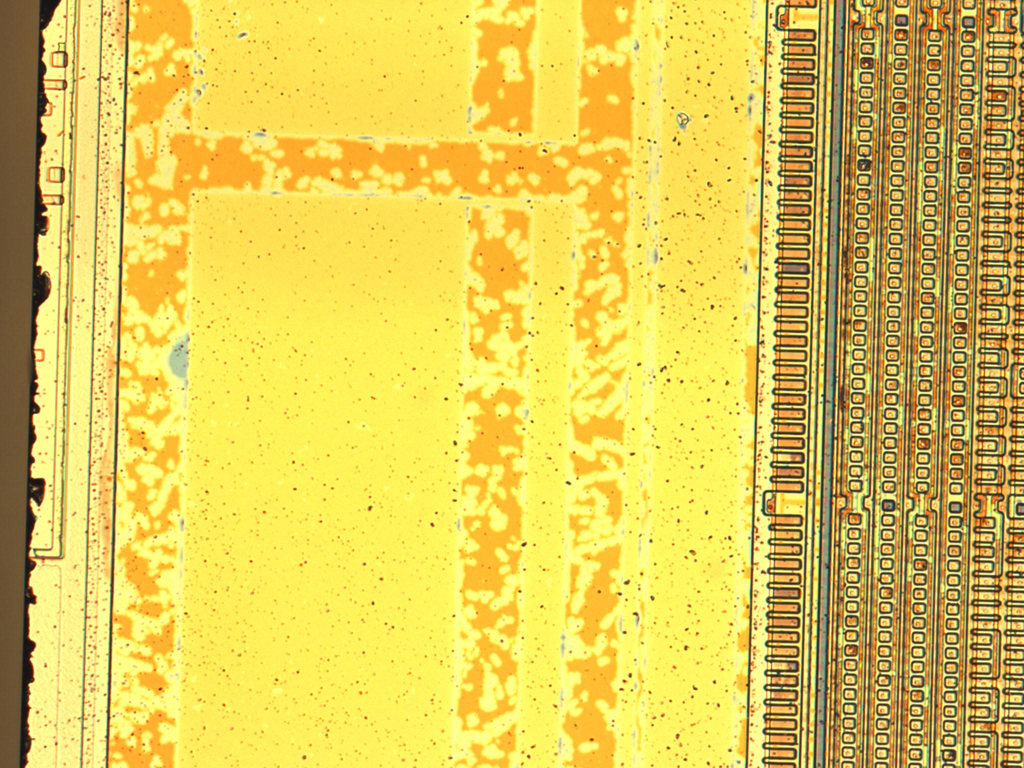
In this picture, the outer eight row lines (polysilicon) here can never "switch on" the connection between those "squares" (the bit line connection points) and ground.
Whereas in this example: http://www.neviksti.com/CIC/tengen2/tengen2_031.jpg
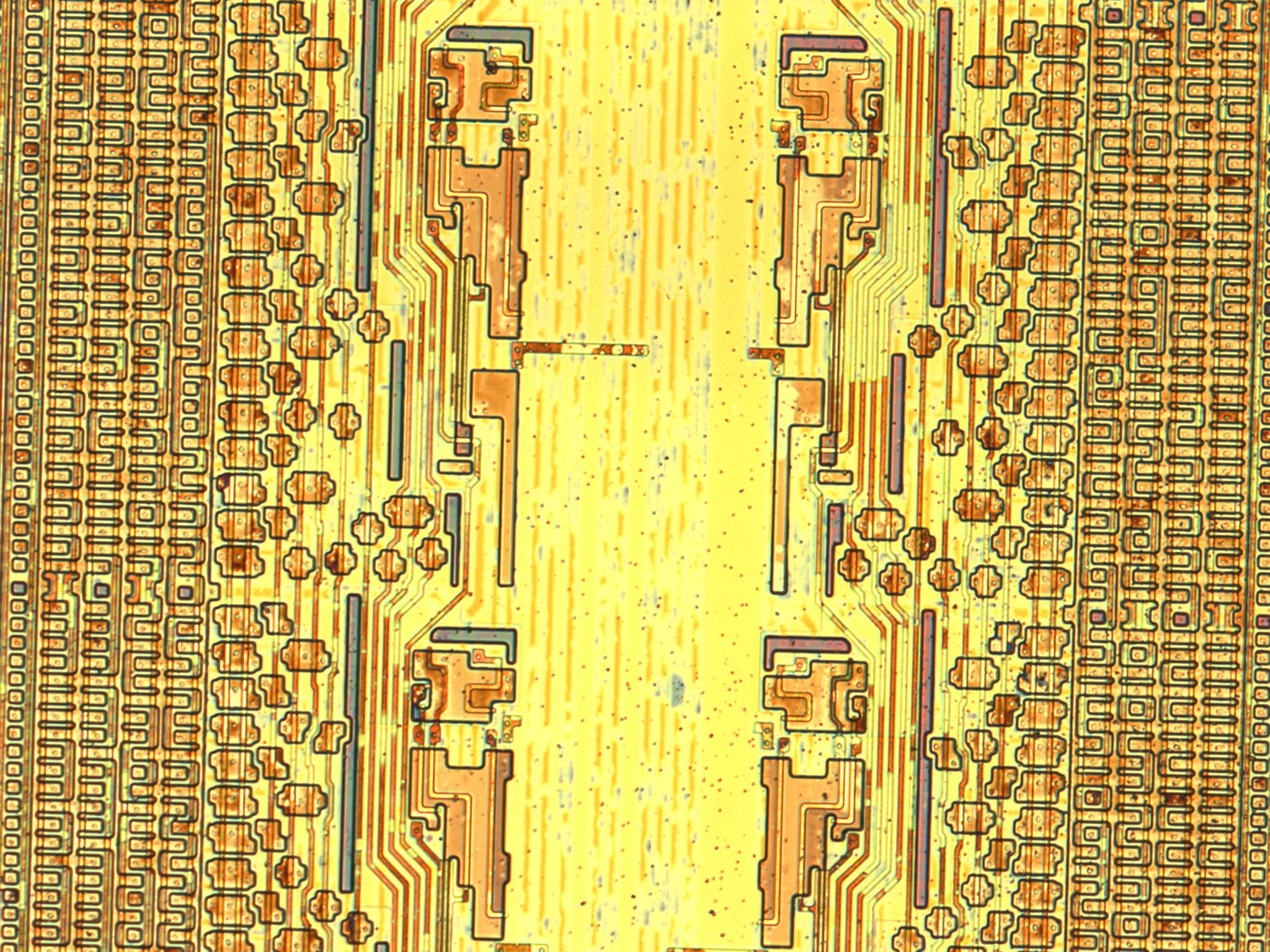
You can see many places where the n-type diffusion layer does butt up against the polysilicon line, so it can act as a transistor.
Does that help some?
.
Since I often get messages asking what the pictures mean, this is probably a good place to pause to explain how to read the pictures. (Kevtris, I'll return to your question in a bit. I kind of got sidetracked.)
All the devices we will be looking at are silicon CMOS devices. This means all the transistors will be FETs. It is not necessary to understand all the details of how the transistor works to be able to "read" these pictures. Here are the basics:
Doped Semiconductors
Pure silicon is not a good conductor, but by putting very small amounts of "impurities" (dopants) in it, it can be made to conduct much better. The amount needed is amazingly small (the number of dopant atoms per silicon atoms can be numbered as parts per billion!).
The silicon can be doped with elements that can donate a free electron or accept/bind an electron. Donor dopants add free electrons to the material which can now drift through it (in the usual terminology: the majority carriers are electrons); this is called n-type silicon because the majority carriers are negative. Acceptor dopants can be thought of as taking an electron from the surrounding material and thus adding an "absence" of an electron (called holes) which can drift through the material (in the usual terminology: the majority carriers are holes); this is called p-type silicon because the majority carriers are positive.
A simple rectifying junction (diode)
If a p-type material is placed next to an n-type material, current can flow fairly easily from p-type to n-type, but for all practical purposes, it can not flow in the other direction.
Remember: The direction of current is defined as the flow of net positive charge. Thus holes can flow from p-type into n-type, and electrons can flow from n-type into p-type. But the reverse processes can be considered non-existent here.
Making a circuit on silicon
A circuit is made by starting with a silicon wafer that is cut from a large single crystal. The crystal is usually grown with some dopants purposely included. For circuits, it is usually lightly p-type.
The surface of the wafer is then patterned with different regions of p or n-type by adding more dopants (diffused or bombarded into the bulk from the surface). I will refer to the actual silicon surface as the "diffusion layer".
Then a pattern of heavily doped polysilicon lines are laid down. These act as interconnects and also as the "gate" for transistors (they control whether the transistor "switches" on or off). I will refer to this as the "polysilicon layer".
The final layer is a metal layer. These act solely as interconnects between the different parts of the circuit. More advanced IC chips have more layers of metal (in analogy to multilayer printed circuit boards).
An FET (Field Effect Transistor)
First, here is what a cross section of a transistor looks like:
http://en.wikipedia.org/wiki/Image:Lateral_mosfet.svg
Notice that the gate is electrically insulated from the silicon surface of the transistor. It is only the electric field from the gate that does the switching (hence the name "Field Effect" transistor).
In that picture, there is n-type material, then p-type (under the gate), and then n-type. If the gate is much more positive than the bulk under the gate, it will pull electrons to the surface. When the surface has excess free electrons, it is effectively an n-type "channel" between the source and drain, so current can flow across. For this reason this transistor is called an n-channel FET (nMOS).
Similarly, we can build an FET with p-type material, then n-type material (under the gate), then p-type material. Now, if the gate is much more negative than the bulk under the gate, it will pull "holes" to the surface. When the surface has excess free holes, it is effectively a p-type "channel" between the source and drain, so current can flow across. For this reason, this transistor is called a p-channel FET (pMOS).
So, an nMOS should have the bulk at GND, and if the gate is at GND (+0V) the transistor is off, and if the gate is at Vcc (+5V), the transistor switches on. In the opposite case, a pMOS should have the "bulk" at Vcc, and if the gate is at Vcc the transistor is off, and if the gate is at GND, the transistor switches on.
Making logic circuits with FETs
Let us look first at the simplest logic gate: an inverter.
http://en.wikipedia.org/wiki/Image:Stat ... verter.png
To read these diagrams, the transistor with the bubble on the gate is pMOS. No bubble on the gate is nMOS.
So let's think it through. Put an input signal of logic 0 (+0V/GND), the pMOS will turn on and the nMOS will turn off. So our output will be connected to logic 1 (+5V/Vcc).
If instead we put an input signal of logic 1 (+5V/Vcc), the pMOS will turn off and the nMOS will turn on. So our output will be connected to logic 0 (+0V/GND).
So if we put in logic 0 the output is logic 1, and if we put in logic 1 the output is logic 0. This is an inverter.
All logic is an expansion upon these ideas. Here is a nice article:
http://en.wikipedia.org/wiki/CMOS
Note in particular the NAND gate, and also look at the physical layer layout that they show as well.
Now for an example with real pictures
If I follow the Clock line, the first thing it does is go to some circuitry to the right of ROM.
Here are the raw pictures I grabbed this example from:
http://www.neviksti.com/CIC/tengen/tengen_42.jpg
http://www.neviksti.com/CIC/tengen2/tengen2_037.jpg
I'll focus on the circuitry the clock signal goes through here.
Here is the circuit with all layers intact:
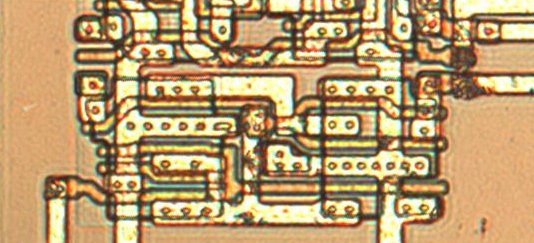
-------------------
Here is the circuit with the metal (and cover oxide) removed:
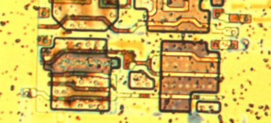
------
Using those two pictures, here is a cartoon version of the bottom layers.
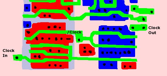
The light red (pink) is the p-type "bulk". The light blue is an n-type "tub like" region that pMOS transistors are put in. For this reason, I often call it the n-well. (Similarly, you could think of the p-type bulk as a p-well.) The dark blue and dark red regions are the more heavily doped source and drain for transistors. The green is polysilicon, and where it crosses the dark blue / dark red are the gate regions. You will also notice dark red squares in pink regions, and dark blue squares in light blue regions. This is done to allow better contact to the metal layer to attach the p-bulk to GND and the n-well to Vcc.
The black dots are where contacts have been made between layers (to the metal layer above in this case). These were highlighted to help people notice what the connections between layers look like in the pictures.
Follow the circuit carefully and you will see that the clock signal is inverted once, then this signal is inverter again (and this final signal is output). So this circuit block is a buffer.
I hope this helps more people understand the pictures.
All the devices we will be looking at are silicon CMOS devices. This means all the transistors will be FETs. It is not necessary to understand all the details of how the transistor works to be able to "read" these pictures. Here are the basics:
Doped Semiconductors
Pure silicon is not a good conductor, but by putting very small amounts of "impurities" (dopants) in it, it can be made to conduct much better. The amount needed is amazingly small (the number of dopant atoms per silicon atoms can be numbered as parts per billion!).
The silicon can be doped with elements that can donate a free electron or accept/bind an electron. Donor dopants add free electrons to the material which can now drift through it (in the usual terminology: the majority carriers are electrons); this is called n-type silicon because the majority carriers are negative. Acceptor dopants can be thought of as taking an electron from the surrounding material and thus adding an "absence" of an electron (called holes) which can drift through the material (in the usual terminology: the majority carriers are holes); this is called p-type silicon because the majority carriers are positive.
A simple rectifying junction (diode)
If a p-type material is placed next to an n-type material, current can flow fairly easily from p-type to n-type, but for all practical purposes, it can not flow in the other direction.
Remember: The direction of current is defined as the flow of net positive charge. Thus holes can flow from p-type into n-type, and electrons can flow from n-type into p-type. But the reverse processes can be considered non-existent here.
Making a circuit on silicon
A circuit is made by starting with a silicon wafer that is cut from a large single crystal. The crystal is usually grown with some dopants purposely included. For circuits, it is usually lightly p-type.
The surface of the wafer is then patterned with different regions of p or n-type by adding more dopants (diffused or bombarded into the bulk from the surface). I will refer to the actual silicon surface as the "diffusion layer".
Then a pattern of heavily doped polysilicon lines are laid down. These act as interconnects and also as the "gate" for transistors (they control whether the transistor "switches" on or off). I will refer to this as the "polysilicon layer".
The final layer is a metal layer. These act solely as interconnects between the different parts of the circuit. More advanced IC chips have more layers of metal (in analogy to multilayer printed circuit boards).
An FET (Field Effect Transistor)
First, here is what a cross section of a transistor looks like:
http://en.wikipedia.org/wiki/Image:Lateral_mosfet.svg
Notice that the gate is electrically insulated from the silicon surface of the transistor. It is only the electric field from the gate that does the switching (hence the name "Field Effect" transistor).
In that picture, there is n-type material, then p-type (under the gate), and then n-type. If the gate is much more positive than the bulk under the gate, it will pull electrons to the surface. When the surface has excess free electrons, it is effectively an n-type "channel" between the source and drain, so current can flow across. For this reason this transistor is called an n-channel FET (nMOS).
Similarly, we can build an FET with p-type material, then n-type material (under the gate), then p-type material. Now, if the gate is much more negative than the bulk under the gate, it will pull "holes" to the surface. When the surface has excess free holes, it is effectively a p-type "channel" between the source and drain, so current can flow across. For this reason, this transistor is called a p-channel FET (pMOS).
So, an nMOS should have the bulk at GND, and if the gate is at GND (+0V) the transistor is off, and if the gate is at Vcc (+5V), the transistor switches on. In the opposite case, a pMOS should have the "bulk" at Vcc, and if the gate is at Vcc the transistor is off, and if the gate is at GND, the transistor switches on.
Making logic circuits with FETs
Let us look first at the simplest logic gate: an inverter.
http://en.wikipedia.org/wiki/Image:Stat ... verter.png
To read these diagrams, the transistor with the bubble on the gate is pMOS. No bubble on the gate is nMOS.
So let's think it through. Put an input signal of logic 0 (+0V/GND), the pMOS will turn on and the nMOS will turn off. So our output will be connected to logic 1 (+5V/Vcc).
If instead we put an input signal of logic 1 (+5V/Vcc), the pMOS will turn off and the nMOS will turn on. So our output will be connected to logic 0 (+0V/GND).
So if we put in logic 0 the output is logic 1, and if we put in logic 1 the output is logic 0. This is an inverter.
All logic is an expansion upon these ideas. Here is a nice article:
http://en.wikipedia.org/wiki/CMOS
Note in particular the NAND gate, and also look at the physical layer layout that they show as well.
Now for an example with real pictures
If I follow the Clock line, the first thing it does is go to some circuitry to the right of ROM.
Here are the raw pictures I grabbed this example from:
http://www.neviksti.com/CIC/tengen/tengen_42.jpg
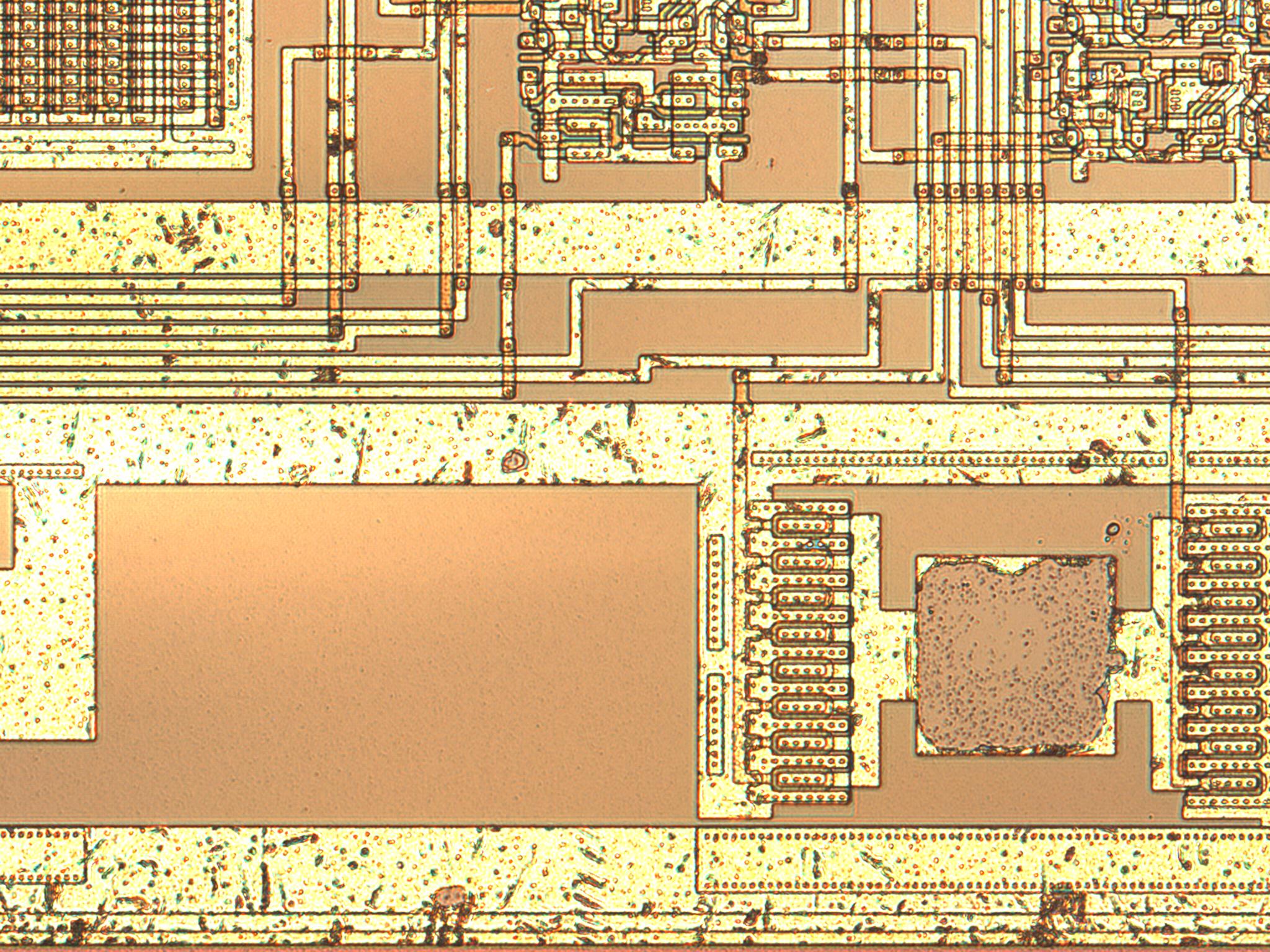
http://www.neviksti.com/CIC/tengen2/tengen2_037.jpg
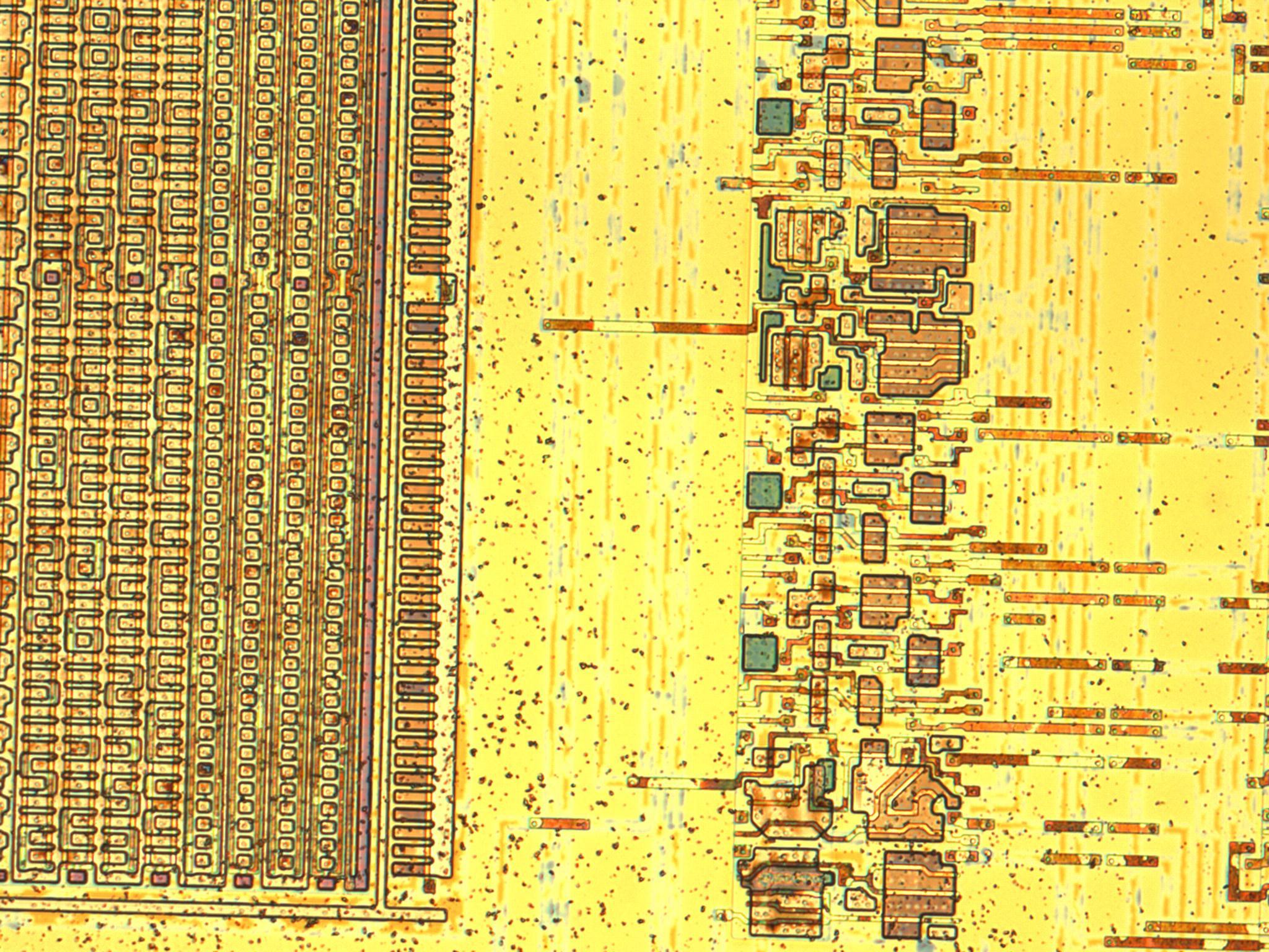
I'll focus on the circuitry the clock signal goes through here.
Here is the circuit with all layers intact:
-------------------
Here is the circuit with the metal (and cover oxide) removed:
------
Using those two pictures, here is a cartoon version of the bottom layers.
The light red (pink) is the p-type "bulk". The light blue is an n-type "tub like" region that pMOS transistors are put in. For this reason, I often call it the n-well. (Similarly, you could think of the p-type bulk as a p-well.) The dark blue and dark red regions are the more heavily doped source and drain for transistors. The green is polysilicon, and where it crosses the dark blue / dark red are the gate regions. You will also notice dark red squares in pink regions, and dark blue squares in light blue regions. This is done to allow better contact to the metal layer to attach the p-bulk to GND and the n-well to Vcc.
The black dots are where contacts have been made between layers (to the metal layer above in this case). These were highlighted to help people notice what the connections between layers look like in the pictures.
Follow the circuit carefully and you will see that the clock signal is inverted once, then this signal is inverter again (and this final signal is output). So this circuit block is a buffer.
I hope this helps more people understand the pictures.
Err.... You mean you CAN understand the working of a circuit by breaking the package and trying to put on paper what is inside ? Looks exiting, but kinda hard and annoying. As long as the CIC contains a microcontroller, I honnestly ask myself what people can figure out with it only by looking CMOS connexions inside.
Bregalad wrote:
As long as the CIC contains a microcontroller, I honnestly ask myself what people can figure out with it only by looking CMOS connexions inside.
As far as processors go, this is very very simple. Yes, it would still take a long time to trace everything out, but hopefully that will not be necessary.
For instance, the ROM bits can be read out easily now. Maybe just by the frequency of opcodes, someone can get good ideas of what they do.
Also, if we can identify parts of the circuit (adder, comparator, register (maybe that is the sole purpose of the SRAM), program counter, etc) then we can understand a lot without tracing every single line.
kevtris wrote:
I just see two things that look the same. I almost need to have it circled. I'm not even sure where the transistors are. There's two types of structures on the left and right, which I'm not sure what they are.
Here's what I was trying to describe with words:
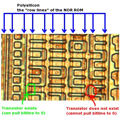
I hope that helps some. It is hard to describe these things.
Anyway, if you browse the pictures, it looks like a sizeable portion of the ROM is unused.
---------------------------
EDIT: I just realized something. Can someone with a logic analyzer setup test a chip that can be key or lock? Keep rerunning the system and pulse the lock/key pin at different times to determine when the CPU checks the pin. This way we can identify the cycle times that certain instructions are ran.
Also, as a side project reverse engineering a different chip, I noticed that observing the current through the GND pin of the chip while the chip ran allowed one to identify loop times and from there roughly determine instructions. If that works for this chip as well, it would be very useful. (Since we also have the rom in this case, it is extra useful.)
I did all that with borrowed equipment, which I don't have access to now. Can one of you fellows with the logic analyzer and oscilloscope look into that for us? I'm really curious to see the results.
.
True, but someone managed to crack the Nintendo DS's lockout, which is as hardware based as you describe.
blargg wrote:
My understanding is that the two CIC chips run identical programs and continually communicate some portion of their state between each other. If these communications differ, the NES goes into reset mode.
Is it complicated a mod to generally disable that kind of reset within the NES itself?
Cybergoth wrote:
Is it complicated a mod to generally disable that kind of reset within the NES itself?
Nope, you just open up the NES and break off the 4th pin of the lockout chip. Then supposedly solder it to GND, but I think most people don't do that step and it seems to be just fine (must be TTL, so that's probably OK).
Memblers wrote:
Cybergoth wrote:
Is it complicated a mod to generally disable that kind of reset within the NES itself?
Nope, you just open up the NES and break off the 4th pin of the lockout chip. Then supposedly solder it to GND, but I think most people don't do that step and it seems to be just fine (must be TTL, so that's probably OK).I see. So generally spoken, the lockout chip is no real showstopper for a simple cartridge release and this discussion is rather of academic interest? Or is that kind of mod rather uncommon within todays userbase?
It is somewhat uncommon. People who import carts will do it, but I think a lot of the more non-technically oriented people don't want to open up their NES and cut stuff in there. There's like a bazillion screws in there (standard phillips thankfully), and armor plating (makes the NES much lighter when removed), heheh, but it's pretty easy otherwise.
On the carts I'll be publishing, I'll be charging $5 for a lockout chip (only North America ones for now) and I'm hoping that'll be a decent incentive for people to clip their chips. It's kind of a hassle to desolder those.
Interestingly, the redesigned NES (top-loading one) doesn't have the lockout chip at all. Nor does the Famicom, in case you didn't know.
Memblers wrote:
It is somewhat uncommon. People who import carts will do it, but I think a lot of the more non-technically oriented people don't want to open up their NES and cut stuff in there. There's like a bazillion screws in there (standard phillips thankfully), and armor plating (makes the NES much lighter when removed), heheh, but it's pretty easy otherwise.
Maybe a few good homebrew game releases would 'talk' more people into doing so
Memblers wrote:
On the carts I'll be publishing,
You're going to start a publishing service?
Memblers wrote:
I'll be charging $5 for a lockout chip (only North America ones for now) and I'm hoping that'll be a decent incentive for people to clip their chips.
Hm... wouldn't non-CIC PCBs be better? Or is it somehow required to cannibalize them anyway?
Memblers wrote:
It's kind of a hassle to desolder those.
I'm thinking of making a modded NES a requirement. Single-Point of Administration one may call it. Instead of keeping the problem alive for generations to come, cut it now once and for all!
Memblers wrote:
Interestingly, the redesigned NES (top-loading one) doesn't have the lockout chip at all. Nor does the Famicom, in case you didn't know.
And European NESes? (NESsi?
Would it be hard to make boards with one of the -5V lockout defeats (e.g. Camerica or Color Dreams) soldered into the CIC holes?
Cybergoth wrote:
So generally spoken, the lockout chip is no real showstopper for a simple cartridge release and this discussion is rather of academic interest?
For small quantity releases (which any release now would be), it is not much of a problem to obtain CIC chips (as for disabling it instead, I think requesting general users to disable the system CIC is a bit unreasonable, but most people involved in homebrew would probably be okay with it). So yes, in that sense this is only of "academic interest".
But, like all others here, I do the things I do because it is an enjoyable hobby. I really like trying to figure out how stuff works, and learning more about hardware along the way. There is a goal in this case (figuring out Nintendo's secret) which makes it even more enjoyable for me, because nothing motivates like an interesting challenge. Of course it is also nice to know that people could "emulate" the CIC chip for a cartridge if we succeed, but it is not the driving force (for me at least).
----------
Anyway, back on topic, the original reason we focussed on the Tengen chip was because we hoped it would be an easier way to get a peek into the algorithm. Unfortunately it appears as custom as Nintendo's chip. It was neat to see the top layers removed, but now that we know we can expose and read the circuitry ... I think I'm going to go back and focus on the actual CIC. If I figure that out, we immediately can understand the code from the CIC of the SNES, NES, and its regional variations. Also, the real CIC appears to be organized better (which may make it easier to identify functional blocks).
Or can someone think of a reason the Tengen might still be easier?
neviksti wrote:
But, like all others here, I do the things I do because it is an enjoyable hobby.
Sure. I can see the challenge for a hardare guy. Being a software guy myself I'm just trying to figure the size of this roadblock
Cybergoth wrote:
You're going to start a publishing service? When will it be on air?
For anyone that has a game (or demo, music disk, etc.) that doesn't do mid-frame CHR bankswitching (or can otherwise tolerate being converted to CHR-RAM, basically), and is smaller than 256kB, then it's available right now.
http://memblers.portabledev.info/pics/board1.jpg
I can make some awesome-looking waterproof labels too (IMHO).
Pretty much any other setups, I can design a new board for in the near future (or now if the game is cool enough, heheh).
Quote:
Hm... wouldn't non-CIC PCBs be better? Or is it somehow required to cannibalize them anyway?
I'm not sure what you mean. It's a pretty negligable cost to reserve the space for one in the crammed into the corner of my new board designs, doesn't always need a chip installed though. For now I'm using cases from SMB/DH carts (which have gloptop chips most of the time), and pulling CICs from my own cart collection.
Quote:
I'm thinking of making a modded NES a requirement. Single-Point of Administration one may call it. Instead of keeping the problem alive for generations to come, cut it now once and for all! 
Yeah, definitely, if we can get people to do it. There's just an insane amount of NES's out there though. Over here, used to seem like one for nearly every household with a kid.
Memblers wrote:
Interestingly, the redesigned NES (top-loading one) doesn't have the lockout chip at all. Nor does the Famicom, in case you didn't know.
Quote:
And European NESes? (NESsi?  )
)
Unfortunately, the regional situation is pretty bad. There's seperate lockout chips for UK (shared with Australia), France, rest of Europe, Hong Kong, North America.. I think. Maybe more or less regions than that.
Memblers wrote:
For anyone that has a game (or demo, music disk, etc.) that doesn't do mid-frame CHR bankswitching (or can otherwise tolerate being converted to CHR-RAM, basically), and is smaller than 256kB, then it's available right now.
Now that's incredibly good news! I'm currently toying with a hopefully (for a beginner) reasonably small project of porting a C64 game that is only 24KB in size, so I'm pretty certain to be able to match your specs
Memblers wrote:
Pretty much any other setups, I can design a new board for in the near future (or now if the game is cool enough, heheh).
Grand Theftendo?
Memblers wrote:
I'm not sure what you mean. It's a pretty negligable cost to reserve the space for one in the crammed into the corner of my new board designs, doesn't always need a chip installed though.
Ah, ok. I feared it'd make things unnecessary complicated/expensive.
Memblers wrote:
There's just an insane amount of NES's out there though. Over here, used to seem like one for nearly every household with a kid.
Almost the same here
Memblers wrote:
Unfortunately, the regional situation is pretty bad. There's seperate lockout chips for UK (shared with Australia), France, rest of Europe, Hong Kong, North America.. I think. Maybe more or less regions than that.
I see. So those special region customers would be required to (preferably) "break the leg" of the problem, or send in their own regional SMB/DH first?
As many NESs that are out there, couldn't you just piggyback a working NES game onto another cart ala Noah's Ark for the SNES? That would avoid modding and having to make a CRC reproduction.
Of course, half the fun is cracking their code.
-Rob
Of course, half the fun is cracking their code.
-Rob
Which is cheapest?
- CIC from a sacrificed board
- -5 V lockout defeat circuit
- Female 72-pin connector
tepples wrote:
Which is cheapest? 1.CIC from a sacrificed board
Carts are ~$0.50-2.00 in bulk and you get a case too. Just takes time to pull the chip from the board.tepples wrote:
2. -5 V lockout defeat circuit
The defeaters need the nes to pulse them, so extra cart hardware for that is needed too. Could be hazardous on top loaders. ~$0.50-1.00 for parts.tepples wrote:
3. Female 72-pin connector
Connectors are ~$7-10 on eBay, and there is no other known oem connector. Making a T connector is not cheap because of the pitch/thickness of nes boards.
Pulling chips from existing carts will likely be the cheapest/best for a while because you get the case too. Once there are enough good games to produce then fabricating cases might be reasonable like Atari homebrew. Quick estimate would be ~$5-10k for the mold, then ~$0.50 per case with 3k minimum. Thats a lot of cases to break even....
With the CIC cracked you could likely use a $0.50 pic chip to replace it.
With the Tengen chip looking custom and not standard motorola core as hoped, I think comparing the different nintendo region chips would be best. The hardware should be the same, with very small differences in the rom. Comparing those might give hints on where the data and where the code might be. I think I supplied neviksti with ~5 different chips, including the two usa versions. I also have an snes cic (d411?) that should again be the same hardware with a possibly different rom. Can anyone confirm that the N64 uses the same cic again?
For those that can understand the gate arrangement, figuring out the rom address/data decoders would be helpful for figuring out the possible instruction set. Also might be interesting to look at the pins that arent used to see if they go anywhere useful.
For those that can understand the gate arrangement, figuring out the rom address/data decoders would be helpful for figuring out the possible instruction set. Also might be interesting to look at the pins that arent used to see if they go anywhere useful.
I don't know the technical details, but I think the N64's CIC is significantly different from the NES and SNES CICs. (Look at the "key code" system used by the N64 GameShark.)
Another thought: grab one of the cic 161 chips from tototek and check it out. I assume they arent using ones ripped from carts... Anyone have a Super Flash cart with one to see whats written on it?
I get my female 72-pin connectors for ~$1 from china, they're connected to family converters (for playing nes games on famicoms), but they're easy to desolder.
bunnyboy wrote:
I think comparing the different nintendo region chips would be best.
Yes, that was the plan at one point. I agree, let's forget about the Tengen for now, and I'll start on those other chips that you sent. I'm not sure what to expect, but I really hope for small changes in the ROM.
For the people that looked at the data sequences with a logic analyzer (or equivalent homebrew):
Did you look at different region CICs? It would be great to have a yeah/neah on whether or not we can expect at least the startup sequence to be the same (ie the begining code to be the same) across all regions.
bunnyboy wrote:
I also have an snes cic (d411?) that should again be the same hardware with a possibly different rom. Can anyone confirm that the N64 uses the same cic again?
Yeah, I looked at a D411 chip. It is the same hardware. I also dumped the ROM and it looked very different to me.
As for the N64, I keep getting requests to look at those. I'm curious, but backlogged at the moment. So maybe down the road we can check into it, but for now I'll try to get the ROM from those other chips (I appologize that this is going so slow).
bunnyboy wrote:
For those that can understand the gate arrangement, figuring out the rom address/data decoders would be helpful for figuring out the possible instruction set.
I can't see how to identify the high address lines from the low address lines just by looking at them. So trying to 100% identify the bit order from the pictures will not be easy (but if we're even considering tracing the logic in the first place, I agree that would be a good place to start).
If I get some good pictures of all the layers, how many feel they would like to help with identifying the logic? If we each choose a section (program counter, instruction decoder, etc) it could go much quicker.
The NES and Super NES CIC use the same hardware with different software. So how much of the data stream is generated by hardware is still an open question, right? So would comparing logic analyzer traces on NES and Super NES CICs help?
I bought one of these a month ago. The chip soldered into where it says the CIC chip is labelled 74LS112 9210.
Is that just a defeater circuit?
.
neviksti wrote:
If I get some good pictures of all the layers, how many feel they would like to help with identifying the logic? If we each choose a section (program counter, instruction decoder, etc) it could go much quicker.
I'd be interested in helping. I have a solid electrical and logic background (EE). I'll have to pick up the VLSI needed as we go.
There were no passives near the "CIC" chip so I guess it must be a fake label to avoid Nintendo's wrath.
Does anyone know which bits are compared and which ones are just space fillers? Is it every Nth bit or is it just randomly spaced?
For those looking at the NES CIC rom, one possible Sharp cpu family is the sm5k3/sm5k4/sm5k5
For those looking at the Tengen CIC, I did a rom map using the latest picts from neviksti. His pictures are at http://neviksti.com/CIC/ but dont pound the website unless you want to help!
The Tengen chip appears to have 384 bytes of NOR rom. The binary output is at http://www.nesmuseum.com/10nes/tengen2rom.txt Next step for someone else to do would be convert to hex, then do something like a histogram and compare to common instruction sets.
I still think comparing the different NES CIC chips will be the best way to figure everything out....
bunnyboy wrote:
For those looking at the NES CIC rom, one possible Sharp cpu family is the sm5k3/sm5k4/sm5k5
For those looking at the Tengen CIC, I did a rom map using the latest picts from neviksti. His pictures are at http://neviksti.com/CIC/ but dont pound the website unless you want to help!
The Tengen chip appears to have 384 bytes of NOR rom. The binary output is at http://www.nesmuseum.com/10nes/tengen2rom.txt Next step for someone else to do would be convert to hex, then do something like a histogram and compare to common instruction sets.
I still think comparing the different NES CIC chips will be the best way to
figure everything out....
This is the requested tasks done, except for instruction set comparison.
http://www.geocities.com/kinglag/nesdev/
RE'd logic cells in the CIC:
http://home.comcast.net/~olimar/NES/CIC/
http://home.comcast.net/~olimar/NES/CIC/
.
.
Very interesting! I was beginning to wonder if any significant advances would ever be made, and it looks like it is.
The nice thing about the new dumps is that we can now see very clearly when bits of data are sent between the two chips, even when both transmitted bits are zero. The Tengen chip's PC consistently points to $5E-61 during each transmission, except for the initialization period, where it points to $1C-1F.
Any known instruction sets with opcode $Cxx indicating "jump to $xx" and $Exx indicating "conditional jump to $xx"?
Known opcodes so far:
110xxxxxxxxx - jump to address 'x', unconditional
111xxxxxxxxx - jump to address 'x', conditional
Addresses are actually 9 bits - the chip is capable of addressing 512 words, but it only uses the lower 256.
Speculation:
010aaaaadddd - maybe loads data 'd' into memory 'a' and register
Further up in the thread, it was deduced that the memory was 128 bits divided into 32 4-bit words. After every '010aaaaadddd' instruction, the 'register' debug output shows the same 'd' value.
In lack of any constructive info to add, I just need to say this: wow! You guys are really great for having come to this point. Seems like this riddle is about to be solved at last... can't wait to see the algorithm documented!
I've just posted some text dumps of kevtris's .BIN files at the following URL:
(URL no longer available)
lock1.txt.bz2 and lock2.txt.bz2 are just direct dumps of the .BIN files, with the bits rearranged into something more legible
tengen.txt.bz2 is a straight text dump of the binary ROM data.
lock1b.txt.bz2 and lock2b.txt.bz2 contain abbreviated dumps of the .BIN files (keeping only every 4th cycle, and dropping the 4 'control signals' which don't appear to reveal anything useful) with the ROM data merged in on each line.
I've uncovered a bit more useful information. I traced pin 3 down to 4 more selectors, each of which connect to the upper signal on a bit of RAM. I then traced the selector connected to the uppermost bit of RAM out to pin 5. A bit of extra tracing linked the lower signal on each RAM bit to a flip-flop input (i.e. the lower signals are outputs), meaning the test pins are showing the memory inputs, or what appears to be ALU output.
Also, 2 of the 'control' signals have been figured out - T0 is read/write, and T1 is memory enable (much like the 6502's R/W and M2 signals).
Using this, I attempted to build a list of instructions in relationship to how they access memory. The first attempt did not yield a useful connection, but then I got the idea of associating the 4 cycles worth of control signals (as well as data) with the previous code word. After doing this, I got a very clear picture of how the opcodes on this chip are arranged.
See the file "io.txt" on my site (linked above) for a mapping of instruction data to memory access behavior - 'R' means read, 'W' means write, and 'Z' means it doesn't appear to access memory at all (perhaps register only). Lock*d.txt takes the above mentioned time shift (pipelining, perhaps?) into account, and indicates what sort of memory access is taking place on each instruction.
From this, it would appear that opcodes are 5 bits wide, leaving 7 bits for operands.
With all the recent finds I now have a pretty good idea of how exactly the CIC works.
1st the lock sends 4 bits. Theese bits are read at approx 1D on the tengen chip. As said before this tells the Key what stream to use.
After that the Key alternates between exchanging a random number of bits with the lock (approx. address 5F), and then a random dead space.
Kevtris if you create more logs of the Tengen Debug data I will be more than happy to process and post them. I would prefer some rather long streams since logging mostly dead space tends to cut down the file to about 1/100th it's size.
The file has more details on the exact timings etc.
http://www.geocities.com/rndlogic/Bit_Transfers.txt
Enjoy
My observations thus far:
The main loop for transmissions starts at address $54 and runs through $6E. When executing the instruction at $6E, the 4-bit data output indicates how many iterations are left for the current transmission. The iterator counts up, with a value of zero indicating no more bits remaining to transfer. Thus, the number of bits needed to transfer is known in advance before the actual transmission takes place. Since the iterator is four bits, no more than 16 bits can be transferred in each direction.
Between transmissions, the code beyond $6E executes and seems to perform some sort of complex arithmetic operation (it's not just idle time - real genuine work is taking place here). I noticed one loop (at $91-94) that seems to be adding 9 to a series of values (presumably in memory). There is one "time-killer" loop at $9D-9E which appears to burn eight instructions worth of time, perhaps a sign that the Tengen chip is able to perform its calculations faster than Nintendo's CIC.
During each transmission, it is possible to see what the Tengen chip is going to send to the master, as well as what the master is about to send the Tengen chip (in other words, the Tengen chip already knows what it's supposed to get). There is a jump instruction pointing to itself (an infinite loop) at $5B (with a branch-over preceding it) that is presumably hit when the result from the master doesn't match.
Here's how to see what bits are about to be transmitted on each iteration through the loop. At instruction $5C (taking into account the pipeline behavior Q mentioned earlier), bit 0 of the output data matches the value the master CIC is going to send. At $5D, bit 0 of the output data matches the value the Tengen chip will send. Here's some examples:
Code:
Time $5C $5D I O
198 3 8 1 0
277 9 9 1 1
356 5 5 1 1
435 2 2 0 0
514 15 1 1 1
593 2 2 0 0
672 0 9 0 1
751 15 15 1 1
830 9 9 1 1
909 9 9 1 1
988 0 0 0 0
1067 9 13 1 1
1146 9 15 1 1
1225 9 9 1 1
1304 7 7 1 1
2384 15 0 1 0
2463 10 11 0 1
198 3 8 1 0
277 9 9 1 1
356 5 5 1 1
435 2 2 0 0
514 15 1 1 1
593 2 2 0 0
672 0 9 0 1
751 15 15 1 1
830 9 9 1 1
909 9 9 1 1
988 0 0 0 0
1067 9 13 1 1
1146 9 15 1 1
1225 9 9 1 1
1304 7 7 1 1
2384 15 0 1 0
2463 10 11 0 1
Here's a look at the data stream with my above findings. In each pair of hex digits, the left digit represents the transmission from lock to key, and the right digit represents the transmission from key to lock. In both cases, bit 0 is the bit actually transferred, with the other three bits being visible only through the Tengen chip's test mode.
Code:
198 38 99 55 22 F1 22 09 FF 99 11 00 9D 9F 99 77
2384 F0 AB F6 4F 4F EC
4849 83 8C C4 E5 14 33 CF 4D
6746 AF EC 4F 16 CA F5 64 6B C2
8458 B5 ED 2C FF AD 8A 2E B9
10601 22 87 FE AB C5 37 19 01 29 32 E5 65 DE 6C 17
13603 50
15283 7F 0B 67 86 9D ED 45 1B 97
17163 42 B5 7F 42 E0 2A 0E D2 4B 02 17 92 08 00
20764 A6 8E
22589 95 7F 9A E2 A2 61 5E FD
25404 6F CB 02 38 57 3C 21 C4 38
26888 A6 36 62 C4 2A AA F3 D6 72 F6 35 2E 65 6E
29475 58 6B 74 A1 5C 9A BE B9 08 DD DF E7 00 42
30934 DD 0B 0F 93 1D 2E 59 C0 32 33 29 61 61 BA 25
32550 E6 23 D5
34124 DD 52 B2 77 A9
35940 D3 D7 70 21 26 DA 38 D1 A6 FC AF 0B EA 08
38881 B6 4B D6 72
39802 0B 32 91 15 C4 EF
42507 68 CB B8
44165 16 28 BE 5C 91 E6 C1 2D
45888 28 EE 83 3F 70 56 7F E4 3B E5
48107 4F E8 B6 CC C8 C7 58 3B 4E 10 4F C1 29 CE F5
50773 13 DC 48 EC A7 7A 7D 76
52340 4A 3B 94 01 F9 5A F3 CB 96 A2 E7 3A A3 BC
55191 5C 36
55948 4E 2B
57035 1B B9 ED EC 8B 94 6C D0 8C 56 06
59583 97 BD D3 96
61008 5D 97
62341 31 61 DD 71 49 09 95
63907 FE 7F 70 D4
65488 57 03 A5 46 93
66746 81 7A 71 D2 BB F6 FC E4 1C D0 32 43 90
69674 FD E0 22 4F 51 EE
72313 29 27 7C C6 F1 83 89 61 AE 1D DF 9D 73 84 66
74343 D3
75579 71 92 FF
.
I made a .pdf of Kevin's schematic for all of you that don't want to download that minotaur of a program. Enjoy.
General instruction format:
AAAAABCDEEEE
AAAAA = Opcode
B = Operand 2 select
0 - RAM Address Latch
1 - Accumulator
C = Operand 1 select
0 - Immediate ROM data
1 - RAM data
D - Update Carry flag? (only for some instructions)
0 - Do Not Update Carry
1 - Update Carry (either from arithmetic operation or from ROM/RAM D0)
EEEE = Immediate ROM data
Notable exceptions:
110xAAAAAAAA - JMP $AA
111xAAAAAAAA - BCC $AA
Quietust wrote:
Notable exceptions:
110xAAAAAAAA - BCC $AA
111xAAAAAAAA - JMP $AA
110xAAAAAAAA - BCC $AA
111xAAAAAAAA - JMP $AA
I think you have those reversed. Opcode 110... should be JMP and 111... should be BCC.
dvdmth wrote:
Opcode 110... should be JMP and 111... should be BCC.
Yes, that's what I said.
.
.
Here's what I've got for a disassembly so far.. not much to see except loops doing mostly-unknown things.
http://www.parodius.com/~memblers/nes/tengen_dis.txt
I'll update it as more stuff gets confirmed.
http://www.parodius.com/~memblers/nes/tengen_dis.txt
I'll update it as more stuff gets confirmed.
001011010010 INC A
01001000DDDD LDA #DDDD
Bit 8 and 7 determine where the result from adder is stored.
00 - Ram and A
10 - Ram
01 - A
11 - Y
I've assigned some letters to a few of the registers
A - Accumulator
R - Ram Block
X - Ram In Latch (latches RAM block data when D10 = 0 and D3 = 1
Y - Ram Adress Pointer
Here is excactly what happens in the first loop:
RAM looks like this after this routine:
You'll notice that this agrees with the Data Coming From the Test Mode. Also the it's showing the output of the adder latch and not the contents of the accumulator. Which makes sense as far as what you would want to see for diagnostic purposes.
01001000DDDD LDA #DDDD
Bit 8 and 7 determine where the result from adder is stored.
00 - Ram and A
10 - Ram
01 - A
11 - Y
I've assigned some letters to a few of the registers
A - Accumulator
R - Ram Block
X - Ram In Latch (latches RAM block data when D10 = 0 and D3 = 1
Y - Ram Adress Pointer
Here is excactly what happens in the first loop:
Code:
00 110000000001 JMP 01 Jumps to 01
01 010110001101 LDY 1101 Loads 1101 to the RAM address Latch
02 011000000100 LDAR 0001 Loads 0001 to the RAM block at 1101 and to the Accumulator
03 001110011010 LDX (Y) then INC Y First The RAM block is Latched, then Y is incremented. This is what affects the Carry Flag
04 001001100000 LDAR A + X Accumulator and RAM in are added, then stored to RAM block and accumulator
05 111000000011 JCC 03 Jump 03 if Carry Cleared
RAM looks like this after this routine:
Code:
00 8
.
.
0D 1
0E 2
0F 4
.
.
0D 1
0E 2
0F 4
You'll notice that this agrees with the Data Coming From the Test Mode. Also the it's showing the output of the adder latch and not the contents of the accumulator. Which makes sense as far as what you would want to see for diagnostic purposes.
Here's the instruction set for the Tengen CPU.
http://www.geocities.com/rndlogic/IA.txt
It's complete except for the last 2 bits of 2 instruction groups. I know they have to deal with the carry in. Also they deal with the Data IN and out of the chip and the Highest bit of the RAM address.
Here's What I have done so far, I'll do the rest tomorrow unless someone else does it first.
Code:
00 110000000001 JMP 01
01 010110001101 LDY 1101
02 011000000100 LDAR 0001
03 001110011010 LDX (Y) then INC Y
04 001001100000 LDAR A + X
05 111000000011 JCC 03
06 001111000100 LDY _A
07 001001000010 LDAR A + 1
08 001111000000 LDY A
09 001100000000 LDR Y
0A 000110100000 LDY X
0B 011000001110 LDAR 0010
0C 101111101100 LDX (0) then LDY A + X
0D 000100000001 LDR 0001
0E 001110010100 LDY _Y set Y4??
I might be mistaken, but it appears opcodes in the form 00xx xxxx x1xx perform an XNOR operation instead of XOR. Whenever the code inverts a value (NOT), it uses this opcode format with one input set to zero. XOR would leave the value unchanged, while XNOR would invert it. Also consider the instruction at ROM $13, which is of this format. My trace shows both inputs being set to $8, and the output of this instruction is $F (corresponding to XNOR, not XOR).
Zack S wrote:
I've assigned some letters to a few of the registers
A - Accumulator
R - Ram Block
X - Ram In Latch (latches RAM block data when D10 = 0 and D3 = 1
Y - Ram Adress Pointer
Here is excactly what happens in the first loop:
RAM looks like this after this routine:
A - Accumulator
R - Ram Block
X - Ram In Latch (latches RAM block data when D10 = 0 and D3 = 1
Y - Ram Adress Pointer
Here is excactly what happens in the first loop:
Code:
00 110000000001 JMP 01 Jumps to 01
01 010110001101 LDY 1101 Loads 1101 to the RAM address Latch
02 011000000100 LDAR 0001 Loads 0001 to the RAM block at 1101 and to the Accumulator
03 001110011010 LDX (Y) then INC Y First The RAM block is Latched, then Y is incremented. This is what affects the Carry Flag
04 001001100000 LDAR A + X Accumulator and RAM in are added, then stored to RAM block and accumulator
05 111000000011 JCC 03 Jump 03 if Carry Cleared
01 010110001101 LDY 1101 Loads 1101 to the RAM address Latch
02 011000000100 LDAR 0001 Loads 0001 to the RAM block at 1101 and to the Accumulator
03 001110011010 LDX (Y) then INC Y First The RAM block is Latched, then Y is incremented. This is what affects the Carry Flag
04 001001100000 LDAR A + X Accumulator and RAM in are added, then stored to RAM block and accumulator
05 111000000011 JCC 03 Jump 03 if Carry Cleared
RAM looks like this after this routine:
Code:
00 8
.
.
0D 1
0E 2
0F 4
.
.
0D 1
0E 2
0F 4
That format is really strange and rather difficult to read. Be aware that you don't need to format the code as if it were 6502 assembly - feel free to format it as "operation operand,operand" like lots of other CPUs do. You also don't need to use two separate "registers" for the RAM address pointer and the RAM at said address - simply use () or [] to denote indirection, as such:
Code:
00 JMP $01
01 MOV P,$D
02 MOV [P].A,$1
03 MOV D,[P++]
04 MOV [P].A,A+D
05 JNC $03
01 MOV P,$D
02 MOV [P].A,$1
03 MOV D,[P++]
04 MOV [P].A,A+D
05 JNC $03
In this case, there are effectively 3 registers - "A" (accumulator), "P" (memory address register, or 'pointer'), and "D" (RAM data latch).
I'm also doing a disassembly. Here's how I'm formatting the results:
Note that this is not intended to be reassembled (if it were, I would've have written it this way).
I am having some trouble with a few opcodes, mainly $809 and $869. Does bit 3 of the opcode have special meaning when bits 7-10 are clear?
Code:
$00 C01 JMP $01
$01 58D Y = 13
$02 604 (Y) = A = Y + 4
$03 39A X = (Y); Y = Y + 1 (update C)
$04 260 (Y) = A = A + X
$05 E03 JNC $03
$06 3C4 Y = ~A
$07 242 (Y) = A = A + 1
$08 3C0 Y = A
$09 300 (Y) = Y
$0A 1A0 Y = X
$0B 60E (Y) = A = Y + 14
$0C BEC X = (0); Y = A + X
$0D 101 (Y) = C
$0E 394 Y = ~Y (update C)
$0F 111 (Y) = C (update C)
Note that this is not intended to be reassembled (if it were, I would've have written it this way).
I am having some trouble with a few opcodes, mainly $809 and $869. Does bit 3 of the opcode have special meaning when bits 7-10 are clear?
dvdmth wrote:
I'm also doing a disassembly. Here's how I'm formatting the results:
Note that this is not intended to be reassembled (if it were, I would've have written it this way).
Code:
$00 C01 JMP $01
$01 58D Y = 13
$02 604 (Y) = A = Y + 4
$03 39A X = (Y); Y = Y + 1 (update C)
(snipped)
$01 58D Y = 13
$02 604 (Y) = A = Y + 4
$03 39A X = (Y); Y = Y + 1 (update C)
(snipped)
Note that this is not intended to be reassembled (if it were, I would've have written it this way).
Unless you're imagining an assembler similar to NESHLA, which uses a more Fortran/ALGOL style syntax. It appears Itanium assembly language (get PDF here) uses a similar syntax, with the = sign appended to the name of the destination register.
Another thing: Is it copyright infringement to conduct this reverse engineering publicly, especially given that the production of the work being reverse engineered was deemed an infringement (Atari Games v. Nintendo) due to Tengen defrauding the US Copyright Office?
tepples wrote:
Another thing: Is it copyright infringement to conduct this reverse engineering publicly, especially given that the production of the work being reverse engineered was deemed an infringement (Atari Games v. Nintendo) due to Tengen defrauding the US Copyright Office?
AFAIK, no it wouldn't be. For one thing Tengen is no longer a company, not sure if that matters or not. But mainly, they weren't sued for the actual reverse engineering, rather the means they used to acquire the info (the patent office deal). But I'm no lawyer either
BootGod wrote:
For one thing Tengen is no longer a company
Tengen's assets are now owned by Midway Games.
I have now programmed a fully working emulator for this chip. Fully working in the sense that it produces the correct output for the bitstream that was posted here earlier.
The binary (for Win32) is available from http://thefox.aspekt.fi/tengen_emu.rar
I'll post the sources later on (after I've cleaned them up a bit) if anybody's interested.
The binary (for Win32) is available from http://thefox.aspekt.fi/tengen_emu.rar
I'll post the sources later on (after I've cleaned them up a bit) if anybody's interested.
So you've got an emulator that runs Rabbit. Cool. Now how hard would it be to translate Rabbit into PIC assembly language? And then can we use the info to make an attack on 10NES itself so that we can understand what differs among the NES regions and between the NES and Super NES?
dvdmth wrote:
I might be mistaken, but it appears opcodes in the form 00xx xxxx x1xx perform an XNOR operation instead of XOR. Whenever the code inverts a value (NOT), it uses this opcode format with one input set to zero. XOR would leave the value unchanged, while XNOR would invert it. Also consider the instruction at ROM $13, which is of this format. My trace shows both inputs being set to $8, and the output of this instruction is $F (corresponding to XNOR, not XOR).
Looks like I overlooked the fact that this circuit uses the same XOR gate as the carry circuitry. I'll update that in the instruction set I made.
dvdmth wrote:
I might be mistaken, but it appears opcodes in the form 00xx xxxx x1xx perform an XNOR operation instead of XOR. Whenever the code inverts a value (NOT), it uses this opcode format with one input set to zero. XOR would leave the value unchanged, while XNOR would invert it. Also consider the instruction at ROM $13, which is of this format. My trace shows both inputs being set to $8, and the output of this instruction is $F (corresponding to XNOR, not XOR).
You are exactly right. The carry flags get SET going into every bit, which does (operand A XOR operand B) XOR (carry)
Which has the effect of XNOR.
I will update my documentation to match.
OK, I have a disassembly now, although it doesn't look necessary anymore since someone can reproduce the bitstream with an emulator. I'll trace through the code to see what the algorithm is - I suspect the international versions use the same algorithm but a different seed.
The code from $00-19 initializes most (but not all) of the lower half of RAM. The code from $1A-26 obtains the 4-bit init code from the master. Next, $27-34 finishes initialization of the lower half of RAM. When that is done, the contents of this half of RAM is copied to the upper half ($35-41), which is then patched to obtain the final init state ($42-4C). When all is said and done, the contents of RAM look like this:
The x's above ($00 and $10) appear to be temp storage and not part of the current pseudorandom seed. The value at $01 (s) is related to (but not equal to) to 4-bit seed value sent by the master. To calculate s, do the following:
1. Assume s0, s1, s2, and s3 are the 4 bits sent by the master, in transmission order.
2. The value s is equal to 2 + (s0*8) + (s1*1) + (s2*2) + (s3*4).
In the lagged stream, s2 and s3 are set, so s = 2 + 2 + 4 = 8.
During transmission, the contents of $07 determines the number of bits sent each way. Subtract this number from 8 (mod 16 of course) to determine the number of bits to transfer. A value of zero is equivalent to a value of 15 (although the chip burns two extra instruction cycles when this happens). The master sends data corresponding to the upper half of RAM ($11-1F), with the Tengen chip sending the lower half ($01-0F). The LSB of each nybble is transmitted only. When fewer than 15 bits are sent, the first nybbles are skipped and the ones at the end are transmitted. Bits are sent in the same order they appear in RAM.
Since $07 starts out set to 9, all 15 nybbles are used in the first transmission ((8 - 9) % 16 == 15).
The code from $00-19 initializes most (but not all) of the lower half of RAM. The code from $1A-26 obtains the 4-bit init code from the master. Next, $27-34 finishes initialization of the lower half of RAM. When that is done, the contents of this half of RAM is copied to the upper half ($35-41), which is then patched to obtain the final init state ($42-4C). When all is said and done, the contents of RAM look like this:
Code:
$00-0F: x s 9 5 2 1 2 9 F 9 1 0 D F 9 7
$10-1F: x 3 9 5 2 F 2 0 F 9 1 0 9 9 9 7
$10-1F: x 3 9 5 2 F 2 0 F 9 1 0 9 9 9 7
The x's above ($00 and $10) appear to be temp storage and not part of the current pseudorandom seed. The value at $01 (s) is related to (but not equal to) to 4-bit seed value sent by the master. To calculate s, do the following:
1. Assume s0, s1, s2, and s3 are the 4 bits sent by the master, in transmission order.
2. The value s is equal to 2 + (s0*8) + (s1*1) + (s2*2) + (s3*4).
In the lagged stream, s2 and s3 are set, so s = 2 + 2 + 4 = 8.
During transmission, the contents of $07 determines the number of bits sent each way. Subtract this number from 8 (mod 16 of course) to determine the number of bits to transfer. A value of zero is equivalent to a value of 15 (although the chip burns two extra instruction cycles when this happens). The master sends data corresponding to the upper half of RAM ($11-1F), with the Tengen chip sending the lower half ($01-0F). The LSB of each nybble is transmitted only. When fewer than 15 bits are sent, the first nybbles are skipped and the ones at the end are transmitted. Bits are sent in the same order they appear in RAM.
Since $07 starts out set to 9, all 15 nybbles are used in the first transmission ((8 - 9) % 16 == 15).
dvdmth can you post the disassembly for us all to see? no reason for us all to disassemble it
thanks
thanks
.
tepples wrote:
Another thing: Is it copyright infringement to conduct this reverse engineering publicly, especially given that the production of the work being reverse engineered was deemed an infringement (Atari Games v. Nintendo) due to Tengen defrauding the US Copyright Office?
Even though i know tepples loves playing the devil's copyright advocate, i thought i would at least say that the most major infringement in all of this is your warranty agreement, when you open up your NES to pull out the CIC.
Pretty sure in the US this is now illegal with the DMCA and it's sections on copyright protection and security/encryption tech. Then again, might be legal under the obsolete tech sections of the DMCA. Not that it matters all that much I think.
gannon wrote:
Pretty sure in the US this is now illegal with the DMCA and it's sections on copyright protection and security/encryption tech. Then again, might be legal under the obsolete tech sections of the DMCA. Not that it matters all that much I think.
I wouldn't think DMCA applies, the CIC isn't protecting any kind of copyrighted work at all. It simply stops the NES from resetting every second, and that's all it does (annoying little bastard that it is).
tepples wrote:
So you've got an emulator that runs Rabbit. Cool. Now how hard would it be to translate Rabbit into PIC assembly language?
Looks like it'll be cutting it close, but I'm confident that there'll be a way. Has to be perfectly synchronized (so a clock source other than the 4Mhz available is out of the question), and the PIC is like the Tengen chip in that it takes 4 clocks per instruction (and some of those Tengen instructions do quite a bit at once). Also on the PIC some instructions (like GOTO and branches) take more than 4 clocks. I imagine it's timed code all the way through. So it'll have to be less of a translation and more of a careful rewrite.
Quote:
And then can we use the info to make an attack on 10NES itself so that we can understand what differs among the NES regions and between the NES and Super NES?
SNES CIC seems to have completely different code, so it's not likely gonna help with that.
Hopefully the NES regions only changed the seed, I guess we'll know once we know the full algorithm.
If it does prove too hard, you could always consider an AVR, where most instructions only take a single clock cycle. And AVRs aren't terribly more expensive than PICs as far as I know.
Using the PLL in a PIC might also be an option, if that won't put the PIC totally out of phase with the CIC.
Even though I'm not very tepples-like when it comes to patents and copyrights, I'd also like a discussion on legal issues. Consider this articles for instance: http://www.gamasutra.com/features/20051111/boyd_01.shtml
"The case involved Nintendo suing Atari for copyright and patent infringement of its “10NES” cartridge authentication system. This system is used by the NES to discern the difference between licensed and unlicensed cartridges. The Federal Circuit upheld a judgment in favor of Nintendo based on the copyright analysis alone. This copyright is still valid and will be for about eighty more years. This is also true for other Nintendo copyright registrations associated with the NES."
In a worst case scenario, a PIC-replica made by anyone who has viewed the info resulting from reverse-engineering might be considered infringing, simply because the reverse-engineering was performed on a product which was considered infringing.
On the other hand, I have a feeling that finding someone who can claim to have reverse-engineered the CIC without having viewed the soon-to-be-publicly available docs won't be entirely impossible in the near future, should it be necessary to enter such legal loopholes.
I am all but an expert on legal issues, so I'd like to hear people's opinions on this. Though maybe we oughta split into another thread for such a discussion...
The C++ source code of the emulator is now included in the RAR-archive I posted yesterday: http://thefox.aspekt.fi/tengen_emu.rar
Please bare in mind my goal when writing this emulator was not to go for 100% compatibility with the actual hardware (because I don't have the skills to do that). So please don't kill me if you find something that's not coherent with the hardware. (If you do, let me know, though, or fix the source code yourself.)
Please bare in mind my goal when writing this emulator was not to go for 100% compatibility with the actual hardware (because I don't have the skills to do that). So please don't kill me if you find something that's not coherent with the hardware. (If you do, let me know, though, or fix the source code yourself.)
Zack S wrote:
dvdmth can you post the disassembly for us all to see? no reason for us all to disassemble it
thanks
thanks
As soon as I can figure out how to post text files, I'll do that. I never had to do anything like that before, so I never found out how.
dvdmth wrote:
As soon as I can figure out how to post text files, I'll do that.
Rename it to .txt and most web hosting services (e.g. Geocities) should allow it. If that doesn't work due to draconian policies against remote loading, you'll need to add a matching file on the server:
Code:
<html><head><title>
Rabbit
</title></head><body>
<h1>Rabbit</h1>
<p>
Rabbit is an emulator of Nintendo's NES lockout chip, developed by Tengen (now Midway Games). <a href="rabbit_disassembly.txt">Get the disassembly of Rabbit</a>
</p>
</body></html>
Rabbit
</title></head><body>
<h1>Rabbit</h1>
<p>
Rabbit is an emulator of Nintendo's NES lockout chip, developed by Tengen (now Midway Games). <a href="rabbit_disassembly.txt">Get the disassembly of Rabbit</a>
</p>
</body></html>
The best way to go would be to either widely distribuate numberous copies of the CIC before Nintendo even knows someone reverse enginered it, and when they'll figure it out it will be too late to find someone responsive for that, or just keep the thing underground and unknown so that Nintendo will never know it has been reverse enginered.
Anyway the thing has dured 20 years, wich is long enough. I see no chance to cause any harm to Nintendo by reverse-enginering it.
Anyway the thing has dured 20 years, wich is long enough. I see no chance to cause any harm to Nintendo by reverse-enginering it.
Translate a description of the algorithm into plain English and publish it. Ideas are not subject to copyright, and the 20 year lag means any patents will have expired.
I feel like an idiot now. I don't have a site where I can upload the file, nor do I feel like setting one up at the moment. I guess it'd be best for me to send it to someone else who can post it. Who wouldn't mind doing that for me?
tepples wrote:
Translate a description of the algorithm into plain English and publish it. Ideas are not subject to copyright, and the 20 year lag means any patents will have expired.
But you can encode any binary sequence into grammatically correct English paragraphs. So is it then illegal to memorize such a paragraph that encodes the binary image of a copyrighted file?
I was talking about writing a comprehensive English description of the 10NES program such that any microcontroller programmer skilled in the art can write a compatible program for a 10NES-compatible key chip. Publishing this information in the United States is almost certainly covered under free speech and/or the interoperability exemption of the DMCA.
On the other hand, if you want to pursue steganography, see Gallery of CSS Descramblers
On the other hand, if you want to pursue steganography, see Gallery of CSS Descramblers
tepples wrote:
I was talking about writing a comprehensive English description of the 10NES program such that any microcontroller programmer skilled in the art can write a compatible program for a 10NES-compatible key chip.
You could just do a search-and-replace of things like "=" to "becomes equal to", add clock cycle info, remove linebreaks, and it'll just be the same thing but harder to read. Seems totally pointless to me.
Also what it says on the site you linked "If code that can be directly compiled and executed may be suppressed under the DMCA, as Judge Kaplan asserts in his preliminary ruling..", we don't even have code that we can directly (or even indirectly) compile and run.
dvdmth, thanks for the disassembly. Saves me a lot of time of having to manually decode instructions, heheh.
Can you clarify the difference between "~" and "!"? If ! is to invert, what is ~?
For example:
$06 3C4 Y = ~A
and
$10 383 Y = Y + !C
Can you clarify the difference between "~" and "!"? If ! is to invert, what is ~?
For example:
$06 3C4 Y = ~A
and
$10 383 Y = Y + !C
In C "!" is logical NOT (!5 == 0) while "~" is one's complement.
Just to be absolutely clear, here's a rewrite using the well-understood XOR:
$06 3C4 Y = A XOR $FF
$10 383 Y = (C XOR 1) + Y
(I'm assuming A is 8 bits and C is a one-bit flag)
$06 3C4 Y = A XOR $FF
$10 383 Y = (C XOR 1) + Y
(I'm assuming A is 8 bits and C is a one-bit flag)
blargg wrote:
Just to be absolutely clear, here's a rewrite using the well-understood XOR:
$06 3C4 Y = A XOR $FF
$10 383 Y = (C XOR 1) + Y
(I'm assuming A is 8 bits and C is a one-bit flag)
$06 3C4 Y = A XOR $FF
$10 383 Y = (C XOR 1) + Y
(I'm assuming A is 8 bits and C is a one-bit flag)
That assumption would be incorrect - A is only 4 bits wide, along with most of the other registers (aside from the RAM address reg and the program counter).
I made a Verilog core of the Tengen CIC chip. So far it seems to work in simulations, i'll test it tomorrow on hardware then release the sources.
first of all, great work every one!
here I'm away from computers for two weeks and you've managed to RE most of the chip O_O
second. on the legal issue.. wouldn't publishing the findings in any country without DMCA solve the issue? ^_^
here I'm away from computers for two weeks and you've managed to RE most of the chip O_O
second. on the legal issue.. wouldn't publishing the findings in any country without DMCA solve the issue? ^_^
It appears that the changes to US copyright law enacted as part of the DMCA aren't as much of a specific issue as some including myself may have made it out to be. Chamberlain v. Skylink, 381 F.3d 1178 (Fed. Cir. 2004), and especially Lexmark Int'l v. Static Control Components, 387 F.3d 522 (6th Cir. 2004). The biggest problem here is ordinary copyright law, which is why I'd like to see a plain-English description of the CIC's operation (call it CIC 101 along with NES 101).
Memblers wrote:
dvdmth, thanks for the disassembly. Saves me a lot of time of having to manually decode instructions, heheh.
Can you clarify the difference between "~" and "!"? If ! is to invert, what is ~?
For example:
$06 3C4 Y = ~A
and
$10 383 Y = Y + !C
Can you clarify the difference between "~" and "!"? If ! is to invert, what is ~?
For example:
$06 3C4 Y = ~A
and
$10 383 Y = Y + !C
I suppose I should have defined the symbols I used. ! is boolean NOT (the carry flag is 1 bit, which by definition is a boolean), while ~ is arithmetic NOT (applied to the full width of a word, in this case 4 bits).
The big problem I had when attemping to convert it to PIC assembly is that the size of all registers aren't all specified. I assume A and X are 4-bit. But what about Y, and C ? C would be carry, but it seems it's not, else Y wouldn't take the value of C, wich make no sense.
Also, how much RAM does the CIC have ? 16-bytes (indexed via Y ?) Does the Y acts as a pointer that is the only chance to write and to read the RAM of the MCU ?
Another problem that comes is that you'd always have to manually truc the accumulator register of a 8-bit to 4-bit, test carry, etc... and that is annoying to do and takes quite some time. I think the best way would be to multiply everything by $10, so that the carry set positionned automatically when shifting from $f0 to $00. But then, direct increment opcodes are a pain to do, because you have to manually add $10. I think we have to trick with swaps, and get the actual index in lower nybble when mostly increments are done, and in upper nybble when mostly additions are done.
Finally, all PIC10Fxxx devies can run at 4MHz, but ONLY on an internal oscillator configuration. And that means the only way to syncronize the 4MHz PIC with the other CIC would be to force the PIC to be the master clock, wich I think isn't possible. So even if both MCUs would run at the exact same speed (4MHz), they wouldn't be syncronized to eachother. I don't know if that is a big issue or not. Even if it isn't after a while both devices could end up being dephased (due to oscillator imprecision) and finally the NES would reset after hours of gameplay (pretty system to limit play-time hehehe). Maybe some tricks with Timer0 could fix this, but that would most certainly require external logic, wich is bad.
So I think at least a PIC12Fxxx or another MCU should be used. I'm not totally sure, though.
Bregalad wrote:
The big problem I had when attemping to convert it to PIC assembly is that the size of all registers aren't all specified. I assume A and X are 4-bit. But what about Y, and C ? C would be carry, but it seems it's not, else Y wouldn't take the value of C, wich make no sense.
Also, how much RAM does the CIC have ? 16-bytes (indexed via Y ?) Does the Y acts as a pointer that is the only chance to write and to read the RAM of the MCU ?
Also, how much RAM does the CIC have ? 16-bytes (indexed via Y ?) Does the Y acts as a pointer that is the only chance to write and to read the RAM of the MCU ?
A and X are 4-bit, yes. Y is also 4-bit. C is 1-bit carry flag. There are no places in the disassembly where Y would take value of C. Instead it's "(Y) = C" which means "save C to address pointed to by Y".
CIC has 32 nibbles of RAM. You can index 16 nibbles with Y, but to access the other 16 you have to set "YH" (the MSB of the 5-bit address) to 1.
Besides using Y, there's no other way to read/write from/to RAM. You can override Y with 0, though, to access the first byte without modifying Y.
A = 4-bit accumulator
X = 4-bit input register
Y = 4-bit address register
YH = upper bit of RAM address (think of it as a bank bit - if set, ALL memory accesses, including address 0 overrde, go to $10-1F)
C = 1-bit carry flag
(Y) = 4-bit RAM data at address (YH<<4) + Y
(0) = 4-bit RAM data at address (YH<<4) + 0
X = 4-bit input register
Y = 4-bit address register
YH = upper bit of RAM address (think of it as a bank bit - if set, ALL memory accesses, including address 0 overrde, go to $10-1F)
C = 1-bit carry flag
(Y) = 4-bit RAM data at address (YH<<4) + Y
(0) = 4-bit RAM data at address (YH<<4) + 0
Okay, I've started to translate the code in PIC assembly (timing aside). It's very annoying because those stupids instructions doesn't make any sense, and you don't have any clue to the meaning of them not technically, but in the software viewpoint. I'm pretty sure by translating the algorithm in a understanding form it could be much better to just rewrite a programm doing the same function, but not all the same instructions !! It would also be much more possible to get syncronous with the PIC, because the same arithmetical functions are much faster on a 8-bit CPU than on a 4-bit CPU, so it would complete the operation faster and will be able to by synchronised with the CIC. But if we just complete the list of instruction we have, that will take much more time because a lot of clamping to 4-bits and various tests have to be done.
Also (Y) = C still does make no sense to me. (Y) is a RAM file, wich is 4-bits from what I understand. C is 1-bit. A 4-bit variable just cannot take the value of a 1-bit variable. This is a nonsense. In my current programm, I just assumed that (Y) = 0001 if C=1 and (Y) = 0000 if C=0, but that's most certainly wrong.
A second thing that doesn't make sense if those "Update C" things. How can C be updated by a XNROR function ? Only an add or substract (maybe increment/decrement) could affect C, logically.
Also, I assume the CIC has actually 32 nybbles of RAM, not 32 bytes. Is YH affected by RESET signal ? It seems to never be initialised.
Anyway here is my assembly file (only the begining of the programm is implemented) :
http://jonathan.microclub.ch/CIC_Clone.asm
Bregalad wrote:
Okay, I've started to translate the code in PIC assembly (timing aside). It's very annoying because those stupids instructions doesn't make any sense, and you don't have any clue to the meaning of them not technically, but in the software viewpoint. I'm pretty sure by translating the algorithm in a understanding form it could be much better to just rewrite a programm doing the same function, but not all the same instructions !! It would also be much more possible to get syncronous with the PIC, because the same arithmetical functions are much faster on a 8-bit CPU than on a 4-bit CPU, so it would complete the operation faster and will be able to by synchronised with the CIC. But if we just complete the list of instruction we have, that will take much more time because a lot of clamping to 4-bits and various tests have to be done.
Yeah. I already began translating the algorithm to C. This way I can easily verify that the algorithm works (by using test input), and also I get the benefit of being able to use Visual Studio's debugging toolset.
It's already pretty tidy
Bregalad wrote:
Also (Y) = C still does make no sense to me. (Y) is a RAM file, wich is 4-bits from what I understand. C is 1-bit. A 4-bit variable just cannot take the value of a 1-bit variable. This is a nonsense. In my current programm, I just assumed that (Y) = 0001 if C=1 and (Y) = 0000 if C=0, but that's most certainly wrong.
In fact that is correct. It all comes down to the fact that CIC only has two operations, ADD and XNOR, which can take up to 3 parameters (including the carry flag). (Y) = C is basically something like (Y) = 0 + C, where dvdmth decided to omit the 0 (a 4-bit immediate).
Bregalad wrote:
Also, I assume the CIC has actually 32 nybbles of RAM, not 32 bytes. Is YH affected by RESET signal ? It seems to never be initialised.
Yeah, nibbles it is, I accidentally said bytes earlier. And I think YH must be 0 when the program starts, otherwise it wouldn't make any sense as far as I've looked in to the code.
thefox wrote:
It's already pretty tidy :) I kinda wonder why they used loops and other crazy constructs to initialize the RAM in the beginning, when they'd probably have got away with less instructions if they used plain "load value", "store value" kind of thing.
Misdirection. Often when dealing with content protection/authentication systems, the code will be written in an archaic manner to try to mislead those trying to crack it. If they used simple "(Y) = immediate" instructions, they could've initialized RAM more efficiently, but that would've made it easier to RE the chip from the ROM data.
thefox wrote:
In fact that is correct. It all comes down to the fact that CIC only has two operations, ADD and XNOR, which can take up to 3 parameters (including the carry flag). (Y) = C is basically something like (Y) = 0 + C, where dvdmth decided to omit the 0 (a 4-bit immediate).
The opcode is $101. Decode it yourself (using the instruction set summary at the beginning of the file with the disassembly) and you'll see how the instruction works. To summarize here, the ALU output goes to (Y) (bits 7-8 = 10), the first input is zero (bits 6 and 9 are clear), the second input is zero (bits 5 and 10 are clear), and the carry-in is set to the carry flag (bits 0-1 are 01 and bits 10-11 are clear). The resulting operation is "(Y) = 0 + 0 + C," or "(Y) = C."
dvdmth wrote:
thefox wrote:
It's already pretty tidy I kinda wonder why they used loops and other crazy constructs to initialize the RAM in the beginning, when they'd probably have got away with less instructions if they used plain "load value", "store value" kind of thing.
Misdirection. Often when dealing with content protection/authentication systems, the code will be written in an archaic manner to try to mislead those trying to crack it. If they used simple "(Y) = immediate" instructions, they could've initialized RAM more efficiently, but that would've made it easier to RE the chip from the ROM data.
Yeah, I thought the same. Still seems a bit strange though, because if they bothered to do that, why did they, for example, have a "test"-mode in the chip? Maybe their code is some kind of direct conversion of Nintendo's code.
dvdmth wrote:
thefox wrote:
In fact that is correct. It all comes down to the fact that CIC only has two operations, ADD and XNOR, which can take up to 3 parameters (including the carry flag).
The opcode is $101. Decode it yourself (using the instruction set summary at the beginning of the file with the disassembly) and you'll see how the instruction works. To summarize here, the ALU output goes to (Y) (bits 7-8 = 10), the first input is zero (bits 6 and 9 are clear), the second input is zero (bits 5 and 10 are clear), and the carry-in is set to the carry flag (bits 0-1 are 01 and bits 10-11 are clear). The resulting operation is "(Y) = 0 + 0 + C," or "(Y) = C."
Thanks for the clarification, but that's irrelevant regarding the original question.
thefox wrote:
dvdmth wrote:
thefox wrote:
I kinda wonder why they used loops and other crazy constructs to initialize the RAM in the beginning
Misdirection.
Yeah, I thought the same. Still seems a bit strange though, because if they bothered to do that, why did they, for example, have a "test"-mode in the chip? Maybe their code is some kind of direct conversion of Nintendo's code.
Could be. Perhaps the "odd" stuff is the stuff that varies per region.
Here is the CIC-algorithm translated to C (with a small stub to enable input from file):
http://thefox.aspekt.fi/Tengen.c
http://thefox.aspekt.fi/Tengen.c
One last thing, how does the X (Ram input register) behave ? Is it just a register, or has it some function assigned to it like the Y register (seems it have but the things isn't very well explained).
WOW! I am gone for awhile and come back to find I've missed most of the fun 
Great work everyone! It is so amazing to see the instruction set figured out from all this. It is everything I hoped for. (I'm really glad those pictures finally paid off ).
Anyway, I don't have much time for anything lately, but am still very interested in all this. So, PLEASE, give some feedback on the following:
== What should be the next step regarding reverse engineering the remaining CICs? ==
1) Should I take the time to make ~ 100 pictures of a NES CIC (like I did for the Tengen one), and since we already have the ROM file for that (from previous work), then figure out the instruction set by a combination of looking at the circuitry and "translation"? (Heck, some translation can be investigated now even.) Please note that removing "just" the metal and oxide layer is difficult, and I cannot garauntee that I can reproduce what I did with the Tengen chip (but I believe I probably can).
2) Read out the ROM of several different region CICs. Then just use comparison, knowledge of the code, and "translation" to figure it out. Please note that this is a destructive process and the circuit can't be looked at later (except the diffusion layer), but the circuits all appear to be the same anyway.
3) A better option that I am overlooking.
Of course in the long run we can try both. This is merely a question of the next step as I still want to help, but have very little free time.
Thanks.
EDIT: Oh, and don't forget: Once the CIC instruction set is known, we get the SNES CIC's for free as well. Some have even suggested the N64 security chips use a similar core, but I haven't checked.
Great work everyone! It is so amazing to see the instruction set figured out from all this. It is everything I hoped for. (I'm really glad those pictures finally paid off
Anyway, I don't have much time for anything lately, but am still very interested in all this. So, PLEASE, give some feedback on the following:
== What should be the next step regarding reverse engineering the remaining CICs? ==
1) Should I take the time to make ~ 100 pictures of a NES CIC (like I did for the Tengen one), and since we already have the ROM file for that (from previous work), then figure out the instruction set by a combination of looking at the circuitry and "translation"? (Heck, some translation can be investigated now even.) Please note that removing "just" the metal and oxide layer is difficult, and I cannot garauntee that I can reproduce what I did with the Tengen chip (but I believe I probably can).
2) Read out the ROM of several different region CICs. Then just use comparison, knowledge of the code, and "translation" to figure it out. Please note that this is a destructive process and the circuit can't be looked at later (except the diffusion layer), but the circuits all appear to be the same anyway.
3) A better option that I am overlooking.
Of course in the long run we can try both. This is merely a question of the next step as I still want to help, but have very little free time.
Thanks.
EDIT: Oh, and don't forget: Once the CIC instruction set is known, we get the SNES CIC's for free as well. Some have even suggested the N64 security chips use a similar core, but I haven't checked.
neviksti wrote:
1) Should I take the time to make ~ 100 pictures of a NES CIC (like I did for the Tengen one), and since we already have the ROM file for that (from previous work), then figure out the instruction set by a combination of looking at the circuitry and "translation"? (Heck, some translation can be investigated now even.) Please note that removing "just" the metal and oxide layer is difficult, and I cannot garauntee that I can reproduce what I did with the Tengen chip (but I believe I probably can).
2) Read out the ROM of several different region CICs. Then just use comparison, knowledge of the code, and "translation" to figure it out. Please note that this is a destructive process and the circuit can't be looked at later (except the diffusion layer), but the circuits all appear to be the same anyway.
2) Read out the ROM of several different region CICs. Then just use comparison, knowledge of the code, and "translation" to figure it out. Please note that this is a destructive process and the circuit can't be looked at later (except the diffusion layer), but the circuits all appear to be the same anyway.
If Nintendo's code is anything like Tengen's, it may be better to figure out the hardware first, so I'd go for option 1 (although I wasn't the one who traced the circuit, nor would I ever want to do something like that). Of course, we'd want the RAM data for the other CIC variations eventually if we ever hope to make CIC clones for them.
I updated my disassembly to take out a couple redundancies and clarify how the carry flag is updated in certain situations. I'll send the update to the same address I sent the first copy.
I decided to rename the X register from "RAM input register" to simply "data register," to clarify that it is completely separate from RAM (its only connection to RAM is that it's the register that receives the result of a RAM load - if the address register (Y) changes after a RAM load, X remains unchanged, something that must be taken into account to understand the code).
Bregalad wrote:
Anyway here is my assembly file (only the begining of the programm is implemented) :
http://jonathan.microclub.ch/CIC_Clone.asm
http://jonathan.microclub.ch/CIC_Clone.asm
Nice work, I was gonna do the same thing, but it seems you've started it already. Maybe I could start translating a later point, if you get burned out before finishing (I doubt it, it's not too big really, heheh). Just let me know so we don't duplicate too much work needlessly.
It's jumping the gun a bit to do this by itself though, the idea kevtris and I both had was that we should start out by keeping the timing and code separate. So to start with and make sure we've got a valid base to start with, we could wire one of the PIC's I/O pins to a lockout chip's clock. Run one emulated instruction, clock the CIC, run another, clock, and so on. So I guess just add a macro at the start or end of every translated instruction, should be no problem.
If that works, then we can start the interesting part of gradually optimizing it so we can do our damnedest to get the timing of the data I/O to line up perfectly. Hopefully we can get it to fit in the 12F509, I think we can, otherwise I'll have to start considering the ATTiny11, which has an attractive price but I'm not too thrilled about building/buying yet another chip programmer and learning another design process when there's so much other stuff to put my time into..
My vote would be option 2, read the rom from the other regions. Assuming only the seed is being changed it should be very easy to pick out the bits that are different and form the seed.
I really think all the algorithm stuff will be figured out entirely from the Tengen chip (and soon!). Having the Nintendo CIC gate layout wont be any help. The Nintendo chip also most likely doesnt have all the awesome internal access from the pins.
I really think all the algorithm stuff will be figured out entirely from the Tengen chip (and soon!). Having the Nintendo CIC gate layout wont be any help. The Nintendo chip also most likely doesnt have all the awesome internal access from the pins.
Members, I've done a lot with the AVR series, and I much prefer the instruction set to that of the PICs. The software is much easier and I would be happy to loan you my STK500 to work on the Tiny11. Going from the 6502's instruction set to the AVR was much easier for me, than the PICs.
AVRs are super easy.
AVRs are super easy.
Quote:
My vote would be option 2, read the rom from the other regions. Assuming only the seed is being changed it should be very easy to pick out the bits that are different and form the seed.
It's just an assumtion. I've another one : Maybe Nintendo did just change the formula between the coded string lenght the main CIC sends and between the actual stirng lenght. (I mean the forumla dvdmth posted on page 12). I think that would be rather a easy way from Nintendo to get totally different data sterams, with the same seed and code, and just a diferent lenght formula.
Quote:
Members, I've done a lot with the AVR series, and I much prefer the instruction set to that of the PICs. The software is much easier and I would be happy to loan you my STK500 to work on the Tiny11. Going from the 6502's instruction set to the AVR was much easier for me, than the PICs.
Maybe so, but from what I just reseached smaller AVR are DIP28, and it would be wastefull to use a chip with so much I/Os for that stupid CIC. I've never programmed any AVR, so I just cannot tell. Effectivly the PIC instruction set has absolutely nothing to do with the 6502 (6502 is much more powerfull in my opinion), but it's just different, and you can easily get used to it. The main difference is that for almost each opperation you have to tell if the result goes to "file" or "W register", so you can do crazy things like incrementing a variable and load it to the W accumulator in one single istruction, and without affecting the original variable. The main problem is that there is no indexed mode, you have no chance to ever do "lda Array,X", you're forced to use indirect adressing or just direct adressing.
Quote:
It's jumping the gun a bit to do this by itself though, the idea kevtris and I both had was that we should start out by keeping the timing and code separate. So to start with and make sure we've got a valid base to start with, we could wire one of the PIC's I/O pins to a lockout chip's clock. Run one emulated instruction, clock the CIC, run another, clock, and so on. So I guess just add a macro at the start or end of every translated instruction, should be no problem.
That would require the PIC's clock to be at least ten times faster than CICs, and maybe even more. Even with a PLL circuit we only can get 4 times faster (form what I got) and with two PLL circuits in series it would be 16 times faster, but the PIC12F509 will never run at a such rate (64MHz). I just think it's better to rewrite the whole algorithm in PIC assembly, and I'm pretty sure the PIC can perform actual calculations much faster than CIC, simply emulating the instuction like I did won't be of much use. I think I'll stop to just emulating instuction on the PIC and I'll try to do my best to understand the actual algorithm. This instruction set is horrible and incredibly confusing, tough. I think I'll work with it.
EDIT : I still have no idea on the behaviour of the X Register, so maybe I'm getting things all wrong. I'm now trying to understand how the first nybble transmission works (the transmition in the initialisation code). However, it's nearly impossible becaue it relies on its reset state, wich is unpredictable, so the state of RAM after initialisation is totally unpredicatable. I don't know if all RAM is supposed to be cleared on powerup, but I don't think so.
Check out the AVR instruction set:
You get 32 registers w/ indirect access using x,y or z registers.
More about the instruction set can be found here:
http://homepage.ntlworld.com/matthew.ro ... rinstr.htm
and
http://www.atmel.com/atmel/acrobat/doc0856.pdf
and
http://en.wikipedia.org/wiki/AVR_instruction_set
You get 32 registers w/ indirect access using x,y or z registers.
More about the instruction set can be found here:
http://homepage.ntlworld.com/matthew.ro ... rinstr.htm
and
http://www.atmel.com/atmel/acrobat/doc0856.pdf
and
http://en.wikipedia.org/wiki/AVR_instruction_set
drk421: Thanks for the great devkit loan offer, I'll give it some thought.
There is an DIP8 one, ATTiny11 is 50 cents from Digikey. 1kB of program memory (not sure about instruction size though), and 32 bytes of RAM, which is barely enough but there a decent amount of registers. But the main reason it's interesting is because it runs 1 instruction per clock, rather than 1 instruction per 4 clocks on the PIC and Tengen chip. It almost allows us to be lazy and translate the code, but surely understanding the algorithm would be much nicer.
Ultimately, the algorithm doesn't matter too much, the lockout chip is all about the timing. It's very possible the CIC will know something is up if we write to it's data-in even once on any clock cycle other than the exactly correct one.
That's not the purpose though, what I mean is all the speed in the world won't make any difference if we don't have the instruction set and execution 100% perfectly accurate. Programming a PIC and sticking it right onto an NES cart as a test would be awesome if it works, it's not impossible and I'd be very impressed, but if it doesn't work it'll be a dead end that's nearly impossible to debug.
I'm just advocating the safe way, taking the CIC out of the NES and letting the PIC clock it at it's own leisurely pace. Eventually it could be whittled down to clock the CIC for every PIC instruction, and then when that works it should be ready to stick onto an NES cart for the real test.
Bregalad wrote:
Maybe so, but from what I just reseached smaller AVR are DIP28, and it would be wastefull to use a chip with so much I/Os for that stupid CIC.
There is an DIP8 one, ATTiny11 is 50 cents from Digikey. 1kB of program memory (not sure about instruction size though), and 32 bytes of RAM, which is barely enough but there a decent amount of registers. But the main reason it's interesting is because it runs 1 instruction per clock, rather than 1 instruction per 4 clocks on the PIC and Tengen chip. It almost allows us to be lazy and translate the code, but surely understanding the algorithm would be much nicer.
Ultimately, the algorithm doesn't matter too much, the lockout chip is all about the timing. It's very possible the CIC will know something is up if we write to it's data-in even once on any clock cycle other than the exactly correct one.
Quote:
That would require the PIC's clock to be at least ten times faster than CICs, and maybe even more.
That's not the purpose though, what I mean is all the speed in the world won't make any difference if we don't have the instruction set and execution 100% perfectly accurate. Programming a PIC and sticking it right onto an NES cart as a test would be awesome if it works, it's not impossible and I'd be very impressed, but if it doesn't work it'll be a dead end that's nearly impossible to debug.
I'm just advocating the safe way, taking the CIC out of the NES and letting the PIC clock it at it's own leisurely pace. Eventually it could be whittled down to clock the CIC for every PIC instruction, and then when that works it should be ready to stick onto an NES cart for the real test.
Quote:
There is an DIP8 one, ATTiny11 is 50 cents from Digikey. 1kB of program memory (not sure about instruction size though), and 32 bytes of RAM, which is barely enough but there a decent amount of registers. But the main reason it's interesting is because it runs 1 instruction per clock, rather than 1 instruction per 4 clocks on the PIC and Tengen chip.
Sound interesting. I think this is a option to be considerated, but I'm pretty sure the PIC can do it as well (just a totally different way to reproduce the same algorithm faster and then kill the remaining time should work fine). There is already places where the Tengin chip kills time to wait Nintendo's one.
EDIT : Looking at the datasheet is doesn't seem that the AVR tigny supports external clock, wich is a pain in the ass, just like the PIC10F series. Maybe there is another variant that does ? (I just looked at the first datasheet that came up, it was ATigny15L)
EDIT 2 : Okay, the ATigny 13 supports external clock it seems.
Quote:
Ultimately, the algorithm doesn't matter too much, the lockout chip is all about the timing. It's very possible the CIC will know something is up if we write to it's data-in even once on any clock cycle other than the exactly correct one.
Well, the NES' part lock CIC is supposed to be the exact same code, so we're supposed to know exactly how they behave. BTW I'm surprised there is just no place where the programm actually reads the lock/key input pin. I think the Tengen chip is key only, and the lock mode was replaced by the test mode. Also, the lock and keys most probably runs the same programm, but with slight differences.
Quote:
I'm just advocating the safe way, taking the CIC out of the NES and letting the PIC clock it at it's own leisurely pace. Eventually it could be whittled down to clock the CIC for every PIC instruction, and then when that works it should be ready to stick onto an NES cart for the real test.
Yeah, that'd be less frustrating to see it don't work with a plain LED or multimeter than with the actual conole, hehe.
Also, I've updated my PIC emulating code above and fixed a lot of things that was wrong. I think it emulates the main thing proprely, but there is probably still errors in the translation. Also I looked at the 18F509 datasheet, and yeah, PLL is supported so that's still an option.
Bregalad wrote:
Well, the NES' part lock CIC is supposed to be the exact same code, so we're supposed to know exactly how they behave. BTW I'm surprised there is just no place where the programm actually reads the lock/key input pin. I think the Tengen chip is key only, and the lock mode was replaced by the test mode. Also, the lock and keys most probably runs the same programm, but with slight differences.
Yeah, it is key only. Also, if you look at my C-translation of the CIC code, you'll see that Tengen chip already does calculate also the "lock" part of the signal. It uses 15 nibbles in the first bank to calculate the "key" part, and 15 nibbles in the second bank to calculate the "lock" part (as dvdmth said in an earlier post). The only reason it reads DATA IN, is to compare its calculations to what the lock is sending. It seems to me that neither the DATA IN values or its internal "lock" calculations matter what it is sending to DATA OUT.
So in short: AFAIK, once it has read the 4-bit ID from lock, it doesn't need the DATA IN at all. But it has to calculate the "lock" data, because the calculations don't run in static time (the time varies based on the calculations). Ie. if it didn't calculate them, it would not be in sync with the lock.
If somebody feels up to it, it would be useful to have longer dumps of conversations between the lock and the key (all variations), than the LOCK2.BIN by kevtris.
Neviksti: I vote for option 1. We still don't understand how the rom is even laid out in the real Nintendo CIC, once that part is figured out (and possibly the instruction decoder and ALU also) then we can get somewhere. Its probably best to image the whole chip so we don't miss anything.
The problem with this is that it takes a long time and is a lot of work for you to snap ~100 pictures of a chip die. So I guess its really up to you.
Lord Nightmare
P.S. I have an SGB-CPU and a PAL SNES CIC if you want to decap those. I also have a few other chips I need decapped but can probably scan myself once the plastic package is removed.
.
That's very interesting. I don't know pretty much how you did it, but it seems like a kinda small timing error or something. Maybe it's just a branch that eats you too much cycles in a main loop or something.
kevtris wrote:
On inspection, 8h was loaded into location 07h... which is the somewhat "special" case where it adjusts the offset from 0 to 1.
I assume you're taking into account the two NOPs that the Tengen chip executes when this condition is true. Make sure you're using up the right amount of time (two instructions = eight cycles) when $07 == 8.
.
I did the disassembly by hand. I double-checked the work by comparing with the logs, and I'm 99% sure I checked every instruction (except for the unimportant ones from $C1-DF). I'll re-check my work, and I invite anyone to find any errors I might've made.
A possibility might be an error in the instruction set description. I placed my interpretation of the instruction set (based mostly on what had already been posted here) at the top of the file. If there are any errors in the instruction set description, that can change the resulting disassembly.
A possibility might be an error in the instruction set description. I placed my interpretation of the instruction set (based mostly on what had already been posted here) at the top of the file. If there are any errors in the instruction set description, that can change the resulting disassembly.
kevtris wrote:
One question- was that disassembly of the lockout data done manually, or was it done using a program? If it was done manually there's a chance some errors were introduced maybe.
My C-translation, on the other hand, was not based on dvdmth's disassembly. Instead I wrote my own disassembler, which disassembled the machine code to some basic C code. Then I iterated over and over those pieces of code, until it was clear enough. So, it is possible my disassembler, and thus the C-translation, is faulty.
As I said earlier, it would be cool to have longer dumps of data of CIC conversations (with different seeds AND different types of chips), so I could test my stuff out with them. So far I've only tested them (the emulator, the output of the disassembler, and the optimized C-algo), with kevtris' LOCK2.BIN, with which they worked flawlessly, but that's not *that* long a dump.
.
.
That's awesome, very nice work.
.
Good job, if it works. I see this PIC available for 0.75 USD in volume, so it's eventually cheaper than buying NTSC U/C donor carts for their CICs.
As I understand it, the next steps are as follows:
As I understand it, the next steps are as follows:
- Build a prototype NROM compatible game PCB that includes this.
- Name this program.
- Figure out the differences among regions.
.
a funny name for that would be misspelled tennis... or "tennes". nothing like a nice parody of 10nes. heheh, just kidding
I'd say bunny just for the rabbit referrence, but that kinda..sucks 
Pretty sweet work though
Pretty sweet work though
Are there any two unique seeds x and y such that f(x) = f(y), where f() is the hashing function? I'm not entirely sure knowledge in this area was good enought back then to where Nintendo would've been able to avoid this.
Quote:
Well, I fit the lockout chip function into an 8 pin PIC12F629 part. So it IS possible for a stock PIC to emulate the lockout chip without any external parts. I didn't have to use an inverter after all to reset the chip.
Well, you're the best hacker in the world definitely.
How did you do it without using an inverter ? Reset signal is high on CIC and low on PICs (and almost all others systems I know). Note that you don't need an integrated inverter if you don't want one, a op-amp with two positive-feedback resistors or one transistor with a base/gate resistor and one pull-up resistor can invert a signal as well easily.
The only other solution I see would be to use internal PIC reset circuit for power-up reset, and enabling positive-edge interrupt on the RESET pin, to manually reset the code. Did you do that ? However, I think it is a lot of trouble (or even impossible) to get both chips in synch on startup.
Now the greatest thing would be to make differences between different regions lockout algorithms, and make a PIC that auto-detecs with wich region chip it's communicating and behave in consequence. Don't know if it's possible, tough.
Quote:
There's 2 free pins on the chip to make a region select or something.
Well, that means different boards for each region and the same crap again. Of course jumper/solder pads could just have the same board configurable for each region, but it would be so cool to have a cart that could just plug in in ANY NES and communicate correctly with the console's security anyway.
Also, I think the PIC12F629 has useless comparator module and EEPROM data (I mean useless to simulate the CIC). Couldn't just the PIC12F509 do well ? I just want that stupid CIC to be emulated with a device wich is just as un-powerfull as possible. Maybe the PIC12F508 could even do, while it has LESS RAM locations than the CIC, that makes overall more bits of RAM than the CIC, because words are 8-bits.
dvdmth wrote:
Are there any two unique seeds x and y such that f(x) = f(y), where f() is the hashing function? I'm not entirely sure knowledge in this area was good enought back then to where Nintendo would've been able to avoid this.
DES was published in 1977, and 10NES was developed seven years later.
.
The 12F509 has two banks of 16 bytes, plus 9 bytes common to both banks, making it 41 bytes overall. Since you can acess whathever bank with the FSR I don't think banks are that much an issue.
I dunno about names, but I've be calling it CIClone (cyclone), like the code posted earlier was named.
Then again...bunny chip...lol
Then again...bunny chip...lol
The name I suggested on IRC last night was the "PICIC", which kevtris found at least slightly amusing.
"CIC-ass chip", anyone?...
I like that. How about CIC-A55, to make it more like a part number?
A55-CIC3R is another in the same style.
A55-CIC3R is another in the same style.
Thus far, I like "CIClone" the best. I don't find much humor in names like "CIC-A55," but that's just my taste (I'm sure I'm in the minority here).
I assume the answer is no, but I'll ask anyway - is it possible to design a clone to fit in a standard CIC socket?
I assume the answer is no, but I'll ask anyway - is it possible to design a clone to fit in a standard CIC socket?
Bananmos wrote:
CIC-ass
Well it does (or it is one), but that's just hee-larious.
blargg wrote:
A55-CIC3R
Now we gotta find some place that'll do acid baths and/or custom logos.
I'm all for "CIClone" too.
The A55-CIC3R name is great, but lets get the discussion back to the fun stuff if we can.
I'm reading up on some newb-ish C tutorials so I can try something. Not sure if it's best way to do it, but.. if the code is the same on the different regions, I (or anyone) could write a little program that would modify the seed values in the Tengen ROM then test the results using thefox's emulator. If (and only if) the code is identical, then I think it should hit a match eventually.
I'm reading up on some newb-ish C tutorials so I can try something. Not sure if it's best way to do it, but.. if the code is the same on the different regions, I (or anyone) could write a little program that would modify the seed values in the Tengen ROM then test the results using thefox's emulator. If (and only if) the code is identical, then I think it should hit a match eventually.
Kevtris (and team!) does it once again.
Is the assembly source for that PIC available?
You never know when those ninja's will show up
Is the assembly source for that PIC available?
You never know when those ninja's will show up
We need to publish it, if only to get the Chinese companies that make SuperCard, M3, and the like interested.
tepples wrote:
We need to publish it, if only to get the Chinese companies that make SuperCard, M3, and the like interested.
Why? If the big established companies need people who actually care about the NES to do their detail work for them so they can make money, that's just lazy.
Memblers wrote:
If the big established companies need people who actually care about the NES to do their detail work for them so they can make money, that's just lazy.
Lazy makes money. Witness the flood of "NoPass" booting cards for the DS once Martin Korth published the description of the crypto used by DS Game Cards in April 2006.
That it does. Watch out, I'm ranting and veering off-topic, heheh. Guess I'm just tired of seeing the concentration of wealth. Gotta have a bunch of cash to actually be able to make more cash, I know if I wasn't so near to broke I'd be producing all kinds of cool stuff myself. I've got no shortage of ideas and even finished designs, that's for sure..
But as far as crazy carts for playing lots of games, I don't think anyone will do a better job than what bunnyboy has been showing. Stuff like that, Tototek, and VGWiz are all cool to me. But I just can't see companies that make flashcarts for new systems in the same light, since they pretty much know and intend for 99% of their users to use their designs for pirating brand new games (which isn't so bad except for the part where they make money off of other people's work, almost as bad as the "recording industry").
But as far as crazy carts for playing lots of games, I don't think anyone will do a better job than what bunnyboy has been showing. Stuff like that, Tototek, and VGWiz are all cool to me. But I just can't see companies that make flashcarts for new systems in the same light, since they pretty much know and intend for 99% of their users to use their designs for pirating brand new games (which isn't so bad except for the part where they make money off of other people's work, almost as bad as the "recording industry").
About the name I trough plain PICIC (evident contraction of PIC and CIC) would do. Another idea would be DISNES, because the 'DIS' would obscurely mean disasembly, disprotected, dissolved, etc... and NES, well, I think it's evident. Also 'DIS' pronunced in french will mean '10' for the parallel with 10NES.
CIClone is cool too, but there is already FPGA called cyclone (I don't think it's an issue however).
Other than this, has the differences between the rabbit chip and the actual CIC has been discovered ? Without this, how would the difference between CICs could be discovered ?
Also, I assume Tengen carts with the rabbit chip in them works only in the U.S. right ?
Memblers wrote:
But I just can't see companies that make flashcarts for new systems in the same light, since they pretty much know and intend for 99% of their users to use their designs for pirating brand new games (which isn't so bad except for the part where they make money off of other people's work, almost as bad as the "recording industry").
You think there isn't a vibrant DS development community on forum.gbadev.org ?
Bregalad: True, Rabbit is designed only for North American NES.
Bregalad wrote:
Other than this, has the differences between the rabbit chip and the actual CIC has been discovered ? Without this, how would the difference between CICs could be discovered ?
Nope, I don't think the rabbit chip has been compared to it much yet (at least not by me). The differences between regions should be easy to spot though, if the number of changed bits matches the # of seed bits, then we know that's all that's changed (and we'd know what bits too). If there's more changes then we'd know how extensively it had changed, though I'd be kinda at a loss at how to continue from there.
Quote:
Also, I assume Tengen carts with the rabbit chip in them works only in the U.S. right ?
Yep, they only released carts in North America.
tepples: I imagined so, thus that 1%.. I have no idea about the quality/quantity of stuff people develop for it, if it's interesting enough to get non-development people interested in getting a flashcart for it though that'd be pretty cool.
Memblers wrote:
tepples: I imagined so, thus that 1%.. I have no idea about the quality/quantity of stuff people develop for it, if it's interesting enough to get non-development people interested in getting a flashcart for it though that'd be pretty cool.
It is. Witness forum.gbadev.org : DS Misc, where numerous users of MoonShell (DS media player), DSLiveWeather (weather.com client), beup (MSN Messenger client), DipStar (cheat tool for commercial Game Cards), and other homebrew productions get their tech support from developers. In fact, we manage to find people who were attracted to the DS scene by piracy and sucker them into the homebrew scene.
.
First of all, I've been gone for a few months and am absolutely blown away by the progress on this. Congratulations and thanks to all those who contributed. I was reading the thread and trying to follow how all this happened. It seems like this is what got the ball rolling:
I'm just curious as to how you figured that out? Was that a result of RE'ing the circuit, or just a random "let's see what this does" thing?
kevtris wrote:
Well, I figured out last night that the Tengen lockout chip has a special test mode you can enter by pulling pin 4 high!
I'm just curious as to how you figured that out? Was that a result of RE'ing the circuit, or just a random "let's see what this does" thing?
The pin 4 thing was figured out from neviksti's second micrograph of the die (after peeling the metal layer off) iirc.
Lord Nightmare
Lord Nightmare
teaguecl wrote:
First of all, I've been gone for a few months and am absolutely blown away by the progress on this. Congratulations and thanks to all those who contributed. I was reading the thread and trying to follow how all this happened. It seems like this is what got the ball rolling:
I'm just curious as to how you figured that out? Was that a result of RE'ing the circuit, or just a random "let's see what this does" thing?
kevtris wrote:
Well, I figured out last night that the Tengen lockout chip has a special test mode you can enter by pulling pin 4 high!
I'm just curious as to how you figured that out? Was that a result of RE'ing the circuit, or just a random "let's see what this does" thing?
I was looking at the die pics and was figuring out what was an input and what was an output pin. That's when I noticed that pins 3 and 4 were inputs, while the other 8 "unused" pins were outputs. I then traced those outputs to the ROM address lines and other various places, via 2 to 1 muxers. The rest kinda fell into place from there. I think Loopy figured out pin 4 was the output enable for those 8 pins.
With dumps of the internal state as it executed, we were well on the way.
.
.
kevtris wrote:
This leaves other countries in europe as a big questionmark, along with Brazil.
I can check which one my brazillian NES has, but as far as I recall, the brazillian NES is identical to the US one, just with an added board to turn the NTSC signal into PAL-M. The main board even has an "NTSC" sticker on it.
tokumaru wrote:
kevtris wrote:
This leaves other countries in europe as a big questionmark, along with Brazil.
I can check which one my brazillian NES has, but as far as I recall, the brazillian NES is identical to the US one, just with an added board to turn the NTSC signal into PAL-M. The main board even has an "NTSC" sticker on it.
Yeah... might be a good idea to look anyways. We've gone through just about every other region and checked now. The other region in question is Korea, but I suspect they use a 3196 like HK and the "asian version" does.
Quote:
For those wondering about the 3199, it runs the coin timing on the Famicombox. When you put money in, it is programmed with the number of minutes of game play you're allowed. When you are getting close to running out of time, it will flash the screen and make a beeping noise out the speaker of your TV for 1 minute. If you do not put more money in, it will then go back to the menu. Interestingly, the beeping and flashing are around the same time interval as the flashing of the red LED on an NES without a cart in it
Definitely not a CIC, but just as stupid usage that those of CICs.
Quote:
This leaves other countries in europe as a big questionmark
All my carts are 3195, most are noted 'FRG' or 'NOE' sometimes there is some other coutry code. (I live in Switzerland, but I think carts are from France and/or Germany. The few box and manuals are in english for older games and in german for newer games). I think 3195 is definitely all PAL territories with 'B' cartridges, while 3197 is all PAL territories with 'A' cartridges (I've never seen any 'A' cartridge arround, tough).
All 3 of my 3 NES' are noted 'FRG' and I think they all have a 3195 in them (since they run 3195 carts).
The 3195 cannot be identical to the 3193, because I've a cart with a 3193 and it don't work in my unmodified console, but does in the one which I've cut pin 4.
Bregalad wrote:
Quote:
For those wondering about the 3199, it runs the coin timing on the Famicombox. When you put money in, it is programmed with the number of minutes of game play you're allowed. When you are getting close to running out of time, it will flash the screen and make a beeping noise out the speaker of your TV for 1 minute. If you do not put more money in, it will then go back to the menu. Interestingly, the beeping and flashing are around the same time interval as the flashing of the red LED on an NES without a cart in it
Definitely not a CIC, but just as stupid usage that those of CICs.
Quote:
This leaves other countries in europe as a big questionmark
All my carts are 3195, most are noted 'FRG' or 'NOE' sometimes there is some other coutry code. (I live in Switzerland, but I think carts are from France and/or Germany. The few box and manuals are in english for older games and in german for newer games). I think 3195 is definitely all PAL territories with 'B' cartridges, while 3197 is all PAL territories with 'A' cartridges (I've never seen any 'A' cartridge arround, tough).
All 3 of my 3 NES' are noted 'FRG' and I think they all have a 3195 in them (since they run 3195 carts).
The 3195 cannot be identical to the 3193, because I've a cart with a 3193 and it don't work in my unmodified console, but does in the one which I've cut pin 4.
Yeah, I meant the 3193 and 3195 appear to use the same algo as each other... with a changed constant or two in the initial hashing loop to set up the seeds, before the 4 bit word is transferred from the lock to the key.
So it looks like 3195 is PAL B, and 3197 is PAL A. That just leaves 3194 as the big unknown.
kevtris wrote:
Only 3193 and 3195 have all 16 seeds. 3197 has 4, and 3198 has 1.
I think the files are misnamed, or there's a typo above. When I parsed the binary files using an app I wrote, 3197.bin had 1 seed and 3198.bin had 4.
Quote:
Yeah, I meant the 3193 and 3195 appear to use the same algo as each other... with a changed constant or two in the initial hashing loop to set up the seeds, before the 4 bit word is transferred from the lock to the key.
That's great. So both of them can definitely be included in a single MCU, that would act like a 3193, and if a reset signal is send a bit later act like a 3195 or something like that.
I think if we could put all 3193, 3195 and 3197 in a single MCU it would be just great ! I don't think 3196 are very common anywhere (since all asian countries uses pirated famiclones instead), and I really don't see how anyone would have use of a famicombox today (with that stupid coin counter). BTW I don't understand why famicombox games were written specially for it... It's not famicom games anymore, if you see what I mean.
Can someone out there check to see if the 3195's timing is consistent with the known hash algorithm? Either I'm doing something wrong (quite likely, as I don't have much confidence in what I'm doing at the moment), or the algorithm timing does not match, in which case the algorithm must have changed. If the algorithm changed, the log data will be virtually useless without a dump of the ROM and better knowledge of the hardware.
I'm hoping I made a mistake here, as I'd much rather see the algorithm unchanged (in which case we easily have enough data to determine the seeds, through brute force if nothing else).
EDIT - It was my mistake. The timing is actually the same for the 3195, so at least that much of the algorithm was left unchanged. Hopefully the rest is unchanged as well....
thefox wrote:
kevtris wrote:
Only 3193 and 3195 have all 16 seeds. 3197 has 4, and 3198 has 1.
I think the files are misnamed, or there's a typo above. When I parsed the binary files using an app I wrote, 3197.bin had 1 seed and 3198.bin had 4.
Yeah sorry, I screwed up. The files are named properly.
I'm in the process of determining the initial seeds for the 3195. Here's what I have so far:
$01 is initialized the same way (2 + 8*s0 + 1*s1 + 2*s2 + 4*s3, where s0-s3 are the seed bits in transmission order).
$02 = 0x7
$03 = 0xB
$04 = 0xD
$07 = 0x9
$0F = 0x7
$11 = 0x1
$12 = 0x7
$13 = 0xB
$14 = 0xE (not 100% sure on this one)
$1F = 0x7
EDIT - added $11-14
I think I've done enough for one day.
I decided to try to crack the "lock" seed (the one in $11-1F, which stays constant regardless of the 4-bit initialization transfer) using a brute-force attack. I only had the program do a small number of hashes (around 8 or so), and to stop if it found more than one match. It didn't take long for a match to be found, and almost immediately thereafter a second one showed up. So I figured I needed a larger data set. I kept adding transmission details (ignoring timing, since I'm only doing one seed by itself), and I kept getting the same results - the same two matches showed up over and over with each test.
I then added a piece of code to output the initial seed and the result of the first hash, as well as the number of cycles required on the actual CIC to complete the job. It turned out both seeds took the same amount of time to hash, and both yielded the exact same result as well. No wonder I wasn't able to narrow down the results by adding additional data.
I may later scan all possible seeds to see how many yield the correct result, and if any take a different amount of time (again, I can't verify accurate timing at this point because I'm only doing half the work the real CIC does). I can verify at the moment that at least 8 different initial seeds can be used, all of which take the same amount of time to hash.
The eight seeds are:
1. $17BEF0AF5706617
2. $17BED2AF5706617
3. $17BEB4AF5706617
4. $17BE96AF5706617
5. $17BE78AF5706617
6. $17BE5AAF5706617
7. $17BE3CAF5706617
8. $17BE1EAF5706617
The result of the first hash is $6EF162D81783986.
Can someone double-check these results? There have been times before when I've made a really dumb mistake in coding that yielded faulty results.
I think I have a working pair of seeds now. The timings match up and everything. I only tested some of the initial 4-bit initialization values, but all of the ones I tested matched all the way through to the end of the logged data, with cycle precision. These are not the only keys that can be used (there are eight possible starting values for each seed, or so it seems).
KEY: $x7BD309F6EF2F97
LOCK: $17BEF0AF5706617
It should now be possible to clone the 3195, assuming the info is accurate.
KEY: $x7BD309F6EF2F97
LOCK: $17BEF0AF5706617
It should now be possible to clone the 3195, assuming the info is accurate.
dvdmth wrote:
I think I have a working pair of seeds now. The timings match up and everything. I only tested some of the initial 4-bit initialization values, but all of the ones I tested matched all the way through to the end of the logged data, with cycle precision.
I tested it with all the 16 seeds now using my C-translation, and it worked flawlessly. Nice work!
I'll begin working on the 3197 once a complete set of data is available (all 16 initializations). It appears the first initialization bit is sent five cycles later than the 3193/3195 (cycle 40 instead of 35). The amount of time between the init transmission and the first seed transmission appears to be the same, but it also appears that $07 is set to an even number, suggesting (if the same formula was used) that it must start out set to 8, which would cause an extra two-cycle delay. Thus, either two fewer cycles occur before the first seed transmission, or the number of bits to transfer is determined in a different way.
I will be able to tell more precisely what is going on as soon as dumps are available for all 16 starting points.
EDIT - I decided to try to work with the 3197 data anyway (mainly from boredom). I may be able to figure out the seeds without having all 16 datasets after all. I have already deduced the values of $01-07, $0F, and $1F (to my own surprise).
In the process, I learned something very interesting. The contents of $07 do NOT affect the number of bits sent at the first transmission. It appears that $07 starts out set to 14 on th 3197, which would mean a submission of only ten bits. However, 15 bits are transmitted in spite of this setting. Subsequent transmissions, however, do appear to use $07 to determine the number of bits to send.
dvdmth wrote:
I think I have a working pair of seeds now. The timings match up and everything. I only tested some of the initial 4-bit initialization values, but all of the ones I tested matched all the way through to the end of the logged data, with cycle precision. These are not the only keys that can be used (there are eight possible starting values for each seed, or so it seems).
KEY: $x7BD309F6EF2F97
LOCK: $17BEF0AF5706617
It should now be possible to clone the 3195, assuming the info is accurate.
KEY: $x7BD309F6EF2F97
LOCK: $17BEF0AF5706617
It should now be possible to clone the 3195, assuming the info is accurate.
Woot! It does indeed work on the real thing. I am testing it with a real 3195 acting as a lock, and it's working nicely.
Great job on finding those seeds so fast! I knew it'd probably be possible, but not that quickly. As for the 3197, I will start dumping it here in a minute once I re-configure my board for dumping.
As for the 3196, I might have a source for a few of those, so we can knock that out if/when I get the chips. I am curious if the 3196 has the same algo as the '3 or '5... or if it's got the newer '7 algo. Only when I get the chips will we know I guess.
I still haven't been able to come up with a source for 3194's yet.
.
Make sure the 3195 seeds remain valid for an extended period of time (at least 24 hours). I noticed that some variations in the seeds take many iterations to show differences. Although the eight "lock" seeds I found are equivalent after the first hash, they did occur within the first 5% or so of all possible combinations, and I have yet to scan the rest to see if there are other possibilities. The ones I found last throughout the dumped data, but I can't rule out the possibility of a differentiation occurring later on. (The "key" seed should have no problems - I was able to scan all possible seed values, which is easier since you know what $07 has to be after each hash).
As for the 3197, I have determined the "key" seed already (need to do some more testing to ensure its accuracy, though). The newly gained knowledge about multiple seeds resulting in the same result after one hash allowed me to find the correct seed very quickly. Unfortunately, the same does not apply to the "lock" seed. It appears the conditions are just wrong to where I can deduce very little from the output data. As a result, unless I can find another method of deduction, I'll have to do a rather extensive brute-force attack on it (the number of unknown bits isn't much larger, but each additional bit doubles the time required for this kind of attack). It may take me days, possibly weeks, before finding a working seed.
I do not plan on working with the 3198, mainly because I see no value in cracking that chip (and besides, a glance at the log suggested to me that it may use completely different code, including a different algorithm). I will certainly do the 3196 and (if it exists) the 3194 when there is data available (after I'm done with the 3197, that is).
dvdmth wrote:
Make sure the 3195 seeds remain valid for an extended period of time (at least 24 hours). I noticed that some variations in the seeds take many iterations to show differences. Although the eight "lock" seeds I found are equivalent after the first hash, they did occur within the first 5% or so of all possible combinations, and I have yet to scan the rest to see if there are other possibilities. The ones I found last throughout the dumped data, but I can't rule out the possibility of a differentiation occurring later on. (The "key" seed should have no problems - I was able to scan all possible seed values, which is easier since you know what $07 has to be after each hash).
I ran probably 10000-20000 frames or more. It was running full bore for probably a half hour. I'm fairly confident it's correct. When one little tiny thing is wrong, the hash magnifies it in just a few iterations. I will do a special extended test of it later.
Quote:
As for the 3197, I have determined the "key" seed already (need to do some more testing to ensure its accuracy, though). The newly gained knowledge about multiple seeds resulting in the same result after one hash allowed me to find the correct seed very quickly. Unfortunately, the same does not apply to the "lock" seed. It appears the conditions are just wrong to where I can deduce very little from the output data. As a result, unless I can find another method of deduction, I'll have to do a rather extensive brute-force attack on it (the number of unknown bits isn't much larger, but each additional bit doubles the time required for this kind of attack). It may take me days, possibly weeks, before finding a working seed.
Yeah, If you need a longer sequence, lemme know and I can generate it. I can generate a specific sequence, or all of them to any length required.
Quote:
I do not plan on working with the 3198, mainly because I see no value in cracking that chip (and besides, a glance at the log suggested to me that it may use completely different code, including a different algorithm). I will certainly do the 3196 and (if it exists) the 3194 when there is data available (after I'm done with the 3197, that is).
Yeah, it'd been nice if it was similar... and I agree that it doesn't have a whole lot of use. Would'a been nice for completeness sake tho
kevtris wrote:
Yeah, If you need a longer sequence, lemme know and I can generate it. I can generate a specific sequence, or all of them to any length required.
There's more than enough data - that's not the problem. The issue is that Nintendo did a better job picking a starting seed. I have improved (slightly) on how many bits I can determine with certainty, so it probably won't take weeks to go through all possibilities remaining, but I still don't have it down to where I'd like it to be.
Bear in mind that it's always possible for my brute-force tester to find the correct answer five seconds after I post this message. Then again, it may be a couple of days before I have it. But, I will have it eventually, and I am committed to finding the seed as quickly as possible.
It's not something where we'll have to run the app on all our PCs like distributed.net, is it?
It wasn't exactly five seconds, but here's a match that runs through the end of the data logs (four init seeds tested):
KEY: x79AA1E0D019D99
LOCK: 558937A00E0D66D
The lock seed definitely needs long-term testing here. I know for a fact that this is not the only possible outcome - others exist that produce different internal results after hashing without affecting the output. It's possible that some bits in the seed are "don't care" bits and never impact the output result (if so, Nintendo really messed up the algorithm), but I will feel much better if my results (for both the 3195 and the 3197) survive at least 24 hours without a hitch. (The issue isn't as big with the key seed, since the restrictions on $07 eliminate most duplicate results very early on, within the first 20 hashes or so).
Be forewarned that the 3197 burns five extra cycles before the initialization phase, and that the first seed transmission is ALWAYS fifteen bits long ($07 has no impact on the first transmission).
.
I am now running the 3197 at full speed. It doesn't seem to have any issues- it works OK. I will let it run for a couple hours, which will be hundreds of thousands of frames. If it still works after that, it most likely is fine.
.
I now realize why I was seeing duplicate results that didn't seem to get resolved with extra data. It appears to be a case of bad luck in terms of the number of times the hash function is executed per frame. The good news is that there's only a small number of cases that need to be tested to ensure every bit to be valid - the problem is waiting for them to occur in the wild. With the "key" seed, it's easy to encounter every case by analyzing the differences between the different initial seedings. For the lock seed, however, it's more difficult to weed out the bad results because you only get one initial seed to work with.
With this new knowledge, I can now safely say that if the chip works for a minute or two, it should never fail afterwards (it'll be practically impossible for a bad bit to slip through the cracks for several seconds, let alone a full minute). Since my findings have now been verified to run for over an hour, I think it's safe to say we have the correct seeds.
Nevertheless, it may not be a bad idea to run multiple long tests, just to make sure nothing weird happens down the line. You never want to run the risk of putting one of these chips in a PowerPak (or whatever), sell it, have the customer play for an hour or so and suddenly have the thing reset unexpectedly (although frankly, I did have that precise issue occur once while playing Blaster Master a few months ago - I guess a speck of dirt interfered or something).
Maybe Nintendo did just not use the 3194 at all, or maybe they just directly jump to the 3195 ?
Anyway, this is GREAT WORK !! Now, almost all consoles (exept asian ones) can definitely be lockless to developpers !
Last thing, is there any hope to have all 3193, 3195 and 3197 in a single chip that will detect wich is the good one ? The lazy way would be to just jump from one programm to the other, so the console will blink one or more time in function of it's region, but will always end up working. A less lazy way could be detecting from where the seed is from, but it definitely looks like hard to do.
Bregalad wrote:
The lazy way would be to just jump from one programm to the other, so the console will blink one or more time in function of it's region, but will always end up working.
That's the exact method kevtris is planning to use, except with one minor modification: you will need to push the reset button multiple times before it will work. The reason is that once the reset light starts flashing, the lockout chip inside the console has completely halted and is no longer listening to the incoming data stream.
It'd also be nice to be able to set a default region with an external jumper. (Although hitting reset a few times isn't that bad)
Will the lockout clone be able to remember which region turned out to be correct, so that the user only has to hit Reset repeatedly the first time it's used? It would be quite annoying if the user had to hit Reset every time he powered up the NES while using this chip.
dvdmth wrote:
Will the lockout clone be able to remember which region turned out to be correct, so that the user only has to hit Reset repeatedly the first time it's used? It would be quite annoying if the user had to hit Reset every time he powered up the NES while using this chip.
From what kevtris has discussed in #nesdev, it sounds like it'll end up working as follows:
- Use the 2 spare pins to select one of 9 valid region settings (each pin can either be GND, VCC, or the PIC's data output signal).
- The first N settings will hardwire the PIC to a specific region.
- The last setting will put the PIC in auto-detect mode.
- When in auto-detect mode, the PIC will switch regions whenever it receives a set number of I/O errors (with only one I/O error detected per reset)
- Once the correct region is found, it is stored in EEPROM until another I/O error is tripped.
Whether or not it ends up being implemented like that is up to kevtris.
.
How will it remember the region? And is there a way to distinguish no comms at all (dirty connector) from failed comms?
The method you describe is fine for me, as long as a faulty transmission doesn't automatically cause the region code that was previously saved to be overwritten with a new value. If a cart fails to boot due to a bad connection, normally a user would power off the console and readjust the cartridge (rather than hit reset). In the event of a power off, any region scanning behavior should be aborted and the last working region selection should be used on the next power on.
dvdmth wrote:
The method you describe is fine for me, as long as a faulty transmission doesn't automatically cause the region code that was previously saved to be overwritten with a new value. If a cart fails to boot due to a bad connection, normally a user would power off the console and readjust the cartridge (rather than hit reset). In the event of a power off, any region scanning behavior should be aborted and the last working region selection should be used on the next power on.
It stores the current region # in EEPROM.
The only way it will store a new region # is if it works for more than 100 or so frames (a few seconds). If it didn't get this far, it won't save the new region #
So yeah if the user powers off, cleans, re-inserts, it will not change regions since last time the cart worked.
Where does it store the state of the currently-being-tried region during region scanning? A second EEPROM location?
BTW, for others asking where the EEPROM is, I believe it's on the PIC chip itself, not an external chip or anything like that.
I second the issue of a dirty connector; having this cause region scanning would reduce success to 1/number of regions, on top of the dirty connector. (How) does it distinguish between failure due to bad connection and failure due to differing region?
blargg wrote:
Where does it store the state of the currently-being-tried region during region scanning?
Presumably, it would be stored in RAM. As long as the chip continues to get power, it'll remember the next region to try.
blargg wrote:
I second the issue of a dirty connector; having this cause region scanning would reduce success to 1/number of regions, on top of the dirty connector. (How) does it distinguish between failure due to bad connection and failure due to differing region?
It won't save the new region until it's successful for a period of time. If your cart connector is dirty and you're adjusting the cart, you'll likely be turning off the NES while adjusting the cart, which will cause it to retry the last successful region each time you turn it back on. On the other hand, if it's failing due to the wrong region, you'll just be hitting the reset button and waiting a few seconds to see if it runs.
At least that's how I understand it.
blargg wrote:
Where does it store the state of the currently-being-tried region during region scanning? A second EEPROM location?
BTW, for others asking where the EEPROM is, I believe it's on the PIC chip itself, not an external chip or anything like that.
I second the issue of a dirty connector; having this cause region scanning would reduce success to 1/number of regions, on top of the dirty connector. (How) does it distinguish between failure due to bad connection and failure due to differing region?
BTW, for others asking where the EEPROM is, I believe it's on the PIC chip itself, not an external chip or anything like that.
I second the issue of a dirty connector; having this cause region scanning would reduce success to 1/number of regions, on top of the dirty connector. (How) does it distinguish between failure due to bad connection and failure due to differing region?
Yeah as Q said, the current region number is stored in a RAM location. The EEPROM is on-chip also, so there are no other chips or parts needed to make this thing work.
You just drop this 8 pin chip on a board and hook it up to the lockout pins and to power, and away you go. There are no other parts required for operation other than a bypass cap across the power pins (which all chips need anyways).
The EEPROM is good for 1 million or more writes, so writing it once when a successful region is found that differs from the stored one will be few and far between. There probably won't be more than 10 writes to it during its lifetime.
oh yeah, forgot to mention it in the last message. I finally know what CIC stands for. It was in one of the patents.... it is short for Checking IC.
Dunno if anyone knew this, but I thought it was quite interesting. I have been wondering what it meant for 10 years now.
Dunno if anyone knew this, but I thought it was quite interesting. I have been wondering what it meant for 10 years now.
This system looks pretty much good, definitely. The only problem if that if the region fail and the power is off then on again, the chip will try the same region over and over, and most people will do that when carts aren't working (regardless of if it's due to dirty connector or invalid region, since both will result in a flickering NES, heh).
well then you got the option to either:
a) Write in the manual for the game how the end-users should operate the cartridge.
or
b) Pre-program the CIC for the buyers region. So it defaults to end-users CIC.
a) Write in the manual for the game how the end-users should operate the cartridge.
or
b) Pre-program the CIC for the buyers region. So it defaults to end-users CIC.
I think I know a good way to use the two remaining pins on the lockout clone. Have them serve as a status indicator of the chip, so that the ROM (through a specially mapped register) can see whether or not the current region selection is valid. The idea would be something like this:
Both outputs should start out set to zero. The chip will set the first output to 1 right after the master CIC releases the reset condition. If the first seed transaction fails, no other changes will be made to the outputs until the next reset. At that time, the chip should clear both outputs until the reset condition is gone, then set the second output to 1. On a subsequent reset, the chip will revert to setting the first output to 1, and so on.
Once a successful seed transaction takes place, the chip should set both outputs to 1. This will remain the setting of the outputs until either (1) the chip is reset or (2) a transaction fails. At that time, behavior should revert to the one described above.
A specially mapped register would be accessible to the PRG-ROM code. On startup, it will check the status of these two bits, and if both are set assume all is well and continue normally. If one bit is set and the other clear, then display a message indicating to the user that the NES should be reset to initialize the cartridge hardware. By keeping track of which of the two bits was set, a game could determine how many times Reset was pressed, and if the count exceeds the number of known regions, a message will inform the user that initialization has failed and that he needs to power off and reinsert the cartridge.
If neither bit is set when the register is polled, then the lockout clone must not be functioning at all. A faulty connection error could then be displayed on the screen.
Mapper hardware can be initialized from these two outputs by taking advantage of the fact that both bits become zero temporarily upon reset. Perform an OR operation between the two outputs, and initialize the hardware on a rising edge of the result.
Obviously, special mapper hardware is necessary to take advantage of these two outputs. I figure, however, that chip will most likely be used on a custom-built cartridge rather that an existing one (which will already have a CIC), so it shouldn't be too hard to design the custom hardware to make use of these outputs.
you're forgetting: if the cic fails, the console will be reset over and over by itself. perhaps a message to power itself off and then on to reset the internal console cic...
Edit: oops, I just realized thats exactly what you implied above. oh well.
Also I think the conclusion was that one pin will be a mapper reset output and the other may be the same thing inverted, and i believe your custom cart could use one of those to basically determine the same thing, whether the cic is failing or passing its transation checks.
That *could* work, because the message in question would just flicker on the screen since the game will boot for about 1 sec before reset. However, if the console has a defeated CIC or has no CIC at all (playing on a famiclone with 72-pins slot or a toploader NES), then the game will refuse to boot due to faliure when communicating with the NES CIC, so you're adding even more stupid copy protection instead of defeating it.
EDIT : I definitely think a power-on reset is a better idea, as long as it still work when no CIC is present in the console. The MMC1 should have an internal power-on reset, since it has a known initial state and it is not connected to the CIC reset line. I don't know about the other mappers, but I guess at least MMC1 and MMC5 aslo have an intenral power-on reset.
EDIT : I definitely think a power-on reset is a better idea, as long as it still work when no CIC is present in the console. The MMC1 should have an internal power-on reset, since it has a known initial state and it is not connected to the CIC reset line. I don't know about the other mappers, but I guess at least MMC1 and MMC5 aslo have an intenral power-on reset.
Then the key will need to indicate a CIC failure due to no communications (either a dirty connector or a toploader) the same way as as a CIC success and let the program on the CPU sort it out. A program can detect the lock-generated soft resets by seeing if resets have happened while the program's copyright screen is still displayed; at least Wisdom Tree games do this while searching for a reset pattern to check against. We'd need one pin for whether a reset button press would change the region.
I take back my suggestion. I see a number of possible faults with the status reporting mechanism as I suggested (e.g. what happens if the CIC in the NES is disabled via pin 4?). I'm not sure if there's any reliable way to utilize these extra pins as outputs for any purpose, since there's no guarantee the chip will even be functional (in a top loader for instance).
Someone I talked to last night did not like the idea of a lockout clone that can work in any region. For one thing, there isn't much value in it since you have to travel from one part of the world to another with the same cartridge before it can have any value over a region-specific CIC. It also complicates usage (particularly for the many people out there who just stick in the cart and start playing without looking at any enclosed documentation). Finally, it requires the game code to detect NTSC vs. PAL and adjust timings of raster effects and/or sound code to match the region.
After having this discussion, I now believe that it is much better for the region select to be hardwired, through the two extra pins on the clone, as was suggested earlier. The region select could be controlled through switches of some kind on the board, if it is desirable to be able to change the region later with minimal effort, but the selection should be made prior to inserting the cart in the NES.
I think it is possible to make games compatible with PAL and NTSC as long as their don't use any raster effect (just simple screen-split using sprite zero hit), and as long as noone cares too much about the music being played at a slightly different pitch and speed. And I don't see much issue for the user as long as the region is stored in EEPROM, he just haves to press reset a few times and I think he'll do it by himself without having to read any doccumentation.
I think it'd be a good idea to have the system being able to be either NTSC only or PAL only (either by using input pins or just by placing a different code inside the PIC). NTSC only means it just have to behave like any U.S. lockout chip (3193). PAL only means it have to alternate between A and B regions (3197 and 3195, possibly 3196).
I think it'd be a good idea to have the system being able to be either NTSC only or PAL only (either by using input pins or just by placing a different code inside the PIC). NTSC only means it just have to behave like any U.S. lockout chip (3193). PAL only means it have to alternate between A and B regions (3197 and 3195, possibly 3196).
dvdmth wrote:
Someone I talked to last night did not like the idea of a lockout clone that can work in any region. For one thing, there isn't much value in it since you have to travel from one part of the world to another with the same cartridge before it can have any value over a region-specific CIC.
That or your cartridge has to travel from the factory to the buyer's part of the world. Or the buyer has to travel to a different part of Europe, which was segmented into separate regions. UK and Italy were in Mattel's "A" market with Australia, and everywhere else in Europe was in the "B" market.
Quote:
It also complicates usage (particularly for the many people out there who just stick in the cart and start playing without looking at any enclosed documentation).
That's why a lot of newer consumer products have a warning label taped over their edge connectors or power connectors.
Quote:
Finally, it requires the game code to detect NTSC vs. PAL and adjust timings of raster effects and/or sound code to match the region.
Unless it's for the different NES regions in different parts of Europe. Besides, some games developed for NTSC could be made PAL tolerant with PPU-timed mappers (like MMC3) for raster effects. Speed is easy to fix: run two world updates in every fifth frame if it detects a PAL machine.
There is even commercial games that have an identical PRG from the USA to PAL regions, not having even the music speed or title screen altered. Kid Icarus is an example, being the only cart I have discovered with the PRGROM marked "NES-KI-PRG" instead of "PAL-XX-PRG".
Is it possible to program the PIC to initialize RAM during the first 15-bit seed transfer, as opposed to earlier? If it can be written that way, then it should be possible to make a lockout clone that works in all parts of Europe without any trial and error. The trick is to take advantage of the different timing between the two regions. The 3197 has an extra delay of 5 instruction cycles before the first 4-bit transfer takes place. For all 4-bit combinations except zero, this is enough to determine which region is appropriate long before the first transmission.
The catch is if the 4-bit transfer is all zero. In this situation, you must wait until the first bit is transferred for the 15-bit transaction. This bit is set to 1 from lock to key and 0 from key to lock. Thus, by seeing when the bit is set to 1, you can determine which region you're in before you need to send a 1 to the lock. However, you'll need to finish RAM initialization while this 15-bit transfer is underway, which might be tricky to pull off. If it can be done, however, then I see no reason why a clone can be set up to work in all parts of Europe without any special end-user operation.
It's not possible, however, to distinguish between the 3193 and 3195 with this technique. I still think the best way to handle this is to have the region selected in hardware (possibly through a switch the user can access) instead of requiring the user to train the chip by pressing Reset if the screen blinks. In an ideal world, user would've replaced their NES cart connectors and kept their cartridges clean, but in the real world this isn't the case, and it can be intimidating if a user has to deal with a blinking screen under circumstances not caused by a bad connection.
Quote:
And I don't see much issue for the user as long as the region is stored in EEPROM, he just haves to press reset a few times and I think he'll do it by himself without having to read any doccumentation.
Remember, the proposed design so far can have the current region changed without any rewiring, so if you're shipping something to region X, you can put the lockout chip into region X before sending it. If the user never uses it outside region X, then it is as if it were hard-wired all along. The automatic region scanning only occurs if the user tries to use it in another region; if there were no automatic, then it wouldn't work at all in this case.
blargg wrote:
Remember, the proposed design so far can have the current region changed without any rewiring, so if you're shipping something to region X, you can put the lockout chip into region X before sending it. If the user never uses it outside region X, then it is as if it were hard-wired all along. The automatic region scanning only occurs if the user tries to use it in another region; if there were no automatic, then it wouldn't work at all in this case.
I suppose that's all right - if the distributor has access to every CIC region and can perform the initialization prior to shipping (this contradicts the earlier point of a cart going directly from a factory to the consumer, but ah well).
Since everyone here seems convinced that a universal, auto-scanning CIC is best, I'll concede. It still would be nice if both European regions can be combined transparently as I described earlier, if for no other reason to reduce the number of region candidates for scanning. It would be particularly nice if the 3196 can be similarly combined with the 3193, to reduce the candidates down to only two (so at most one Reset press would be necessary), but we'll have to wait for the 3196 data, obviously, before reaching any conclusions.
I think it would be pretty well to have a NTSC 3193 clone, and a PAL 3195/3196/3197 clone that would detect the region from the first seed gived. Since 3197 has only a single seed possible I think that will keep things simpler and I don't know if it's needed to emulate the 3696 at all, since it's very not common (asian countries uses famiclones). So just 3195/3197 in a chip would already be a good work.
Bregalad wrote:
I think it would be pretty well to have a NTSC 3193 clone, and a PAL 3195/3196/3197 clone that would detect the region from the first seed gived. Since 3197 has only a single seed possible I think that will keep things simpler and I don't know if it's needed to emulate the 3696 at all, since it's very not common (asian countries uses famiclones). So just 3195/3197 in a chip would already be a good work.
The 3197 has 16 initial seeds just like the others. The original dump kevtris made only had 1 seed because the 3197's timing was different and his dumper didn't correctly interpret the 4-bit seed transfer. The fact that the 3197's timing is offset is why I believe it should be possible to support both the 3195 and the 3197 transparently in one chip.
Depending on the 3196's timing, it may or may not be possible to integrate it with the other region(s) in a transparent fashion. I'm hopeful that it can be, but until data is available there's no way to know.
Can those 2 PIC pins be used as input?
Would there be enough time between resets for the NES CPU to be initialized enough to read the contoller status?
And send that to the PIC?
Instead of a 'auto-switch' method.
Just print:
For Region XYZ Hold A when powering up.
For Region ABC Hold B when powering up.
For Auto mode Hold Select
You could even put that text message in there
(1 second is not very long to read, anyhow)
I don't think that would be possible. Bear in mind that the communication between the lock and key begins before the CPU's /RESET line is released, and once an error occurs the screen blinks on and off indefinitely until the Reset button is pressed (i.e. no second chances).
.
dvdmth wrote:
I don't think that would be possible. Bear in mind that the communication between the lock and key begins before the CPU's /RESET line is released, and once an error occurs the screen blinks on and off indefinitely until the Reset button is pressed (i.e. no second chances).
But the CPU does run while the screen is blinking. It's long enough to detect the PPU speed, read the controllers, and pass on what region to try next time.
Autodetect 60 Hz timing: Ignore buttons and try NTSC
Autodetect 50 Hz timing, holding A: Try PAL-A
Autodetect 50 Hz timing, holding B: Try PAL-B
If you're american that's great, but if you're european like me you don't want to press the button each time you turn on your NES. This would work as long as the A/B button is stored in EEPROM.
If you had to push buttons it couldn't be a drop in replacement module for the original CIC.
kyuusaku wrote:
If you had to push buttons it couldn't be a drop in replacement module for the original CIC.
The Nintendo CIC was produced in at least four variants. We are not trying to create a drop-in replacement; we are trying to create a key chip that is more flexible than the Nintendo CIC. If we wanted to make a drop-in replacement, we would just write one region to the chip's nonvolatile memory at manufacture time.
What's wrong with an auto-scanning drop-in replacement? Requiring a PIC<->NES interface will greatly increase software overhead and infinitely increase hardware overhead in an NROM application. More importantly it will ensure incompatibility with all legacy homebrew and discourage people from using it in favor of a Nintendo CIC.
kyuusaku wrote:
What's wrong with an auto-scanning drop-in replacement?
We're trying to minimize the amount of user interaction in order to get it to decide whether to retry the same region or switch to a different region as of the next power-on, as people don't read manuals.
Quote:
What's wrong with an auto-scanning drop-in replacement? Requiring a PIC<->NES interface will greatly increase software overhead and infinitely increase hardware overhead in an NROM application.
I doubt kevtris will require that your program interact with the chip, rather simply allow it to do so in order to reduce the time taken by auto-detection. I imagine the chip will serve three levels of use, the higher ones being more desirable to the end-user:
1) Basic: chip is pre-configured for a particular region and works as if were the real thing
2) Auto-scanning: chip will determine correct region after multiple power-cycles, without any help from the NES program
3) User-assisted: instructions appear on screen for user to hold certain buttons based on their region
Further, I imagine that all three levels will be served by the same chip and software program, with each being implemented in a way that doesn't conflict with the others. If this is the case, the programmer and producer of the cartridge can decide what level to use.
I've started working on the 3196 data. I was worried for a moment when the timing of the first 15-bit transmission seemed to be different, but it actually is the same (the first transmissions are zero for half of the seed possibilities). I don't think it will take long to crack this one (based on early findings), but I can't say for sure until I have the seeds.
Can someone explain to me how pressing buttons on the controller can simplify the region select processs? Even with this method, the user must press Reset after pressing (and holding) the correct button for the region of choice. Assuming the 3195 and 3197 are combined into one region selection, it will take no more than two resets to set the correct region if auto-detect were used, and pressing Reset twice is simpler to me than reading a blinking message, holding down a button, and pressing Reset.
Can someone explain to me how pressing buttons on the controller can simplify the region select processs? Even with this method, the user must press Reset after pressing (and holding) the correct button for the region of choice. Assuming the 3195 and 3197 are combined into one region selection, it will take no more than two resets to set the correct region if auto-detect were used, and pressing Reset twice is simpler to me than reading a blinking message, holding down a button, and pressing Reset.
dvdmth wrote:
I've started working on the 3196 data. I was worried for a moment when the timing of the first 15-bit transmission seemed to be different, but it actually is the same (the first transmissions are zero for half of the seed possibilities). I don't think it will take long to crack this one (based on early findings), but I can't say for sure until I have the seeds.
Can someone explain to me how pressing buttons on the controller can simplify the region select processs? Even with this method, the user must press Reset after pressing (and holding) the correct button for the region of choice. Assuming the 3195 and 3197 are combined into one region selection, it will take no more than two resets to set the correct region if auto-detect were used, and pressing Reset twice is simpler to me than reading a blinking message, holding down a button, and pressing Reset.
Can someone explain to me how pressing buttons on the controller can simplify the region select processs? Even with this method, the user must press Reset after pressing (and holding) the correct button for the region of choice. Assuming the 3195 and 3197 are combined into one region selection, it will take no more than two resets to set the correct region if auto-detect were used, and pressing Reset twice is simpler to me than reading a blinking message, holding down a button, and pressing Reset.
Yeah, I'm not too fond of that idea myself. I think auto region detection is the way to go. I only have 8 pins on the chip, and 6 are used right off the bat for lockout functionality. The user will have to press reset anyways to try out the change, so I don't see where it is useful to press some "chord" of buttons on the controller.
That implies that there is a way to get data TO the chip from the NES which is easier said than done (you'd need at least 2 bits of output from a latch or whatever to do this).
I could go with an 18 pin chip but then it's kinda big. The 8 pinner was cute 'cause it was half the size of the original.
I think my original plan I came up with was pretty bulletproof and will be agreeable to the end user.
Oh btw, the "Asian version" NES units are PAL. The chips in the Tetris carts I bought were NES-EI-0 for CHR (which is the same as NTSC) and PAL-EI-0 for the PRG. Nothing too strange about that; I suspect most PAL carts are like that.
Crud. I forgot to make up a 6113 set of lockout data. It might be interesting to see what it does differently. I should set that up tonight and upload it, along with a 6113 and a 3193 communicating.
Well, the next CIC I looked at had a different layout. I was not expecting this since even the SNES CIC had the same layout as the NES one in the US. However, the processor + circuitry, on cursory inspection, appears the same (same rom, same ram, some pieces just moved around)... don't underestimate the word cursory in there though
Something changed drastically in the processing as well. I had a VERY hard time staining the ROM. Different regions stained than last time, and the ROM region seemed unaffected. After some fiddling I eventually managed to delineate the ion implantation regions.
Check it out here:
3195A from france
http://www.neviksti.com/CIC/3195A/
Since many of the algorithms are known now, I'm hoping we can reverse engineer the actual instruction code ... and then we get the SNES CIC code for free as well!
3196 results (five seeds tested):
LOCK: 06AD70AF6EF666C
KEY: x6ADCF606EF2F97
This wasn't as smooth as I hoped it would be. A dumb typo led me to a different answer for key, which I didn't catch until after I found the lock seed and started testing different 4-bit starting points. For a moment I thought the 4-bit transmission had to affect more than one nybble, until I realized that my key result was inaccurate to begin with (it eventually went astray even in the dataset I used to get the key seed). Hopefully I didn't make any more typos and the seeds I have here are correct.
I guess I'm only human after all....
dvdmth wrote:
3196 results (five seeds tested):
LOCK: 06AD70AF6EF666C
KEY: x6ADCF606EF2F97
This wasn't as smooth as I hoped it would be. A dumb typo led me to a different answer for key, which I didn't catch until after I found the lock seed and started testing different 4-bit starting points. For a moment I thought the 4-bit transmission had to affect more than one nybble, until I realized that my key result was inaccurate to begin with (it eventually went astray even in the dataset I used to get the key seed). Hopefully I didn't make any more typos and the seeds I have here are correct.
I guess I'm only human after all....
LOCK: 06AD70AF6EF666C
KEY: x6ADCF606EF2F97
This wasn't as smooth as I hoped it would be. A dumb typo led me to a different answer for key, which I didn't catch until after I found the lock seed and started testing different 4-bit starting points. For a moment I thought the 4-bit transmission had to affect more than one nybble, until I realized that my key result was inaccurate to begin with (it eventually went astray even in the dataset I used to get the key seed). Hopefully I didn't make any more typos and the seeds I have here are correct.
I guess I'm only human after all....
Yep, it appears to work! great job on the seed finding mission. I will let it run all night at full speed to see what happens. It made it through about 10 minutes so far, so I'm confident it is correct.
Now that all 4 seeds have been found, the fun part of making the universal chip begins.
I just want to lay some praise on the ad-hoc team here for their work. It's like watching a surgical team work on a patient or something like Mission Impossible, with each specializing in a particular task so that the sum is greater than anyone could have done alone.
Just a quick update- the 3196 is still running many hours later, so I'm pretty sure we got it licked. I may work tonight on the universal chip.
.
Some questions:
1. What happens if there is no CIC in the NES (as is the case with a top loader)? I suspect the PIC won't run wince there's no 4 MHz clock. If the "lockout functioning" pin were polled in this case, would it read back as 0 or 1?
2. What happens if the CIC in the NES is disabled via pin 4 (i.e. the master CIC is in key mode)? Will the PIC function at all? Can the PIC detect this condition?
The important thing here is to keep a game utilizing the "lockout functioning" output from thinking there's a lockout error when in reality there is no lockout functionality to begin with.
3. How will you distribute the final result?
.
kevtris wrote:
When I say "connects to pin X of lockout chip" I mean the chip that would be on the cartridge. Not the chip in the system.
You can distinguish them by calling the chip in the console the "lock chip" and the chip in the cart the "key chip".
kevtris wrote:
/force NTSC - pulling this pin low forces the chip into NTSC only (3193 only) mode. The three PAL modes are not usable. Floating (disconnecting) this pin allows the chip to try all 4 regions.
When is this pin read?
dvdmth wrote:
The important thing here is to keep a game utilizing the "lockout functioning" output from thinking there's a lockout error when in reality there is no lockout functionality to begin with.
The CPU should know that it hasn't reset by the time the game's copyright screen disappears.
tepples wrote:
kevtris wrote:
When I say "connects to pin X of lockout chip" I mean the chip that would be on the cartridge. Not the chip in the system.
You can distinguish them by calling the chip in the console the "lock chip" and the chip in the cart the "key chip".
kevtris wrote:
/force NTSC - pulling this pin low forces the chip into NTSC only (3193 only) mode. The three PAL modes are not usable. Floating (disconnecting) this pin allows the chip to try all 4 regions.
When is this pin read?
It is read a little while after startup. It is designed to be tied low (to pin
Aww man, I was wishing it could tie in with CPU-based 50/60 detection.
It is a very cool thing you eventually DID it !!!
Congratulations !
Congratulations !
I take back my quick comments about the 3195A (pictures of the ROM can be seen at http://neviksti.com/CIC/3195A/ ). It turns out the ROM layout is quite different. It went from the 512 bytes of the 6113 (and SNES D411) to 768 bytes (the bitline decoders went from 1 of 8 to 1 of 12).
Also, there is now a clear pattern in the ROM (unlike before).
The Tengen CIC only used about 256 instructions (12bit each), yes? While the NES CIC has the ROM output 8 bits and has at least 512 of these "instructions". So something seems awefully strange here.
The Tengen chip executed one instruction every 4 clock cycles. Maybe the NES CIC does as well, but there are two 8bit loads involved in this ... maybe first 8 bits is instruction code, and last 8 bits are data. The only time all 8 bits of data should be needed are for jump statements... so maybe we can test this idea.
I finished depackaging the 3193A (from USA) chip tonight, but haven't had time to look at it in the microscope yet. I'm hoping the chip layout will match the 3195A so we can directly compare the ROM data.
What is functionally different between the 3193 and 6113? Can one act as a key/lock and the other only as a key? I'm not sure what to make of the large changes in layout between them as I was not expecting to see that (especially considering they didn't even change the layout when going from 6113 -> SNES D411).
neviksti wrote:
I take back my quick comments about the 3195A (pictures of the ROM can be seen at http://neviksti.com/CIC/3195A/ ). It turns out the ROM layout is quite different. It went from the 512 bytes of the 6113 (and SNES D411) to 768 bytes (the bitline decoders went from 1 of 8 to 1 of 12).
Also, there is now a clear pattern in the ROM (unlike before).
The Tengen CIC only used about 256 instructions (12bit each), yes? While the NES CIC has the ROM output 8 bits and has at least 512 of these "instructions". So something seems awefully strange here.
The Tengen chip executed one instruction every 4 clock cycles. Maybe the NES CIC does as well, but there are two 8bit loads involved in this ... maybe first 8 bits is instruction code, and last 8 bits are data. The only time all 8 bits of data should be needed are for jump statements... so maybe we can test this idea.
I finished depackaging the 3193A (from USA) chip tonight, but haven't had time to look at it in the microscope yet. I'm hoping the chip layout will match the 3195A so we can directly compare the ROM data.
What is functionally different between the 3193 and 6113? Can one act as a key/lock and the other only as a key? I'm not sure what to make of the large changes in layout between them as I was not expecting to see that (especially considering they didn't even change the layout when going from 6113 -> SNES D411).
Also, there is now a clear pattern in the ROM (unlike before).
The Tengen CIC only used about 256 instructions (12bit each), yes? While the NES CIC has the ROM output 8 bits and has at least 512 of these "instructions". So something seems awefully strange here.
The Tengen chip executed one instruction every 4 clock cycles. Maybe the NES CIC does as well, but there are two 8bit loads involved in this ... maybe first 8 bits is instruction code, and last 8 bits are data. The only time all 8 bits of data should be needed are for jump statements... so maybe we can test this idea.
I finished depackaging the 3193A (from USA) chip tonight, but haven't had time to look at it in the microscope yet. I'm hoping the chip layout will match the 3195A so we can directly compare the ROM data.
What is functionally different between the 3193 and 6113? Can one act as a key/lock and the other only as a key? I'm not sure what to make of the large changes in layout between them as I was not expecting to see that (especially considering they didn't even change the layout when going from 6113 -> SNES D411).
I tested this the other day.
the following combinations work:
3193L 3193K
3193L 6113K
6113L 6113K
this combination DOES NOT WORK:
6113L 3193K
L and K are lock/key resp.
This must be why even the last front loaders made in the 90's had 3193's for the locks, long after all the carts were using 6113's.
Just on a side note, when cutting pin 4, this makes the CIC behave as a key and the reset line is freed. So the 6113 most probably act like a key only version of the 3193 (saving costs ?). The combination 6113L 6113K most likely works, beacuse the 6113 acts like a defeated CIC.
Now, about the PIC12 version of the CIC, I'd like to have more prection about the /ForceNTSC pin. You mean it's an open collector input ? What will happen when it is tied high ? The same as if it is floating, the chip will go in all modes, while in Force NTSC mode, is just behave like a 6113 without asking questions ?
Now, about the PIC12 version of the CIC, I'd like to have more prection about the /ForceNTSC pin. You mean it's an open collector input ? What will happen when it is tied high ? The same as if it is floating, the chip will go in all modes, while in Force NTSC mode, is just behave like a 6113 without asking questions ?
Bregalad wrote:
Just on a side note, when cutting pin 4, this makes the CIC behave as a key and the reset line is freed. So the 6113 most probably act like a key only version of the 3193 (saving costs ?). The combination 6113L 6113K most likely works, beacuse the 6113 acts like a defeated CIC.
Now, about the PIC12 version of the CIC, I'd like to have more prection about the /ForceNTSC pin. You mean it's an open collector input ? What will happen when it is tied high ? The same as if it is floating, the chip will go in all modes, while in Force NTSC mode, is just behave like a 6113 without asking questions ?
Now, about the PIC12 version of the CIC, I'd like to have more prection about the /ForceNTSC pin. You mean it's an open collector input ? What will happen when it is tied high ? The same as if it is floating, the chip will go in all modes, while in Force NTSC mode, is just behave like a 6113 without asking questions ?
It is an input, but it has a pullup built into the chip so it's pulled high internally. The internal resistor is around 100K or so. I measured the pin when it's floating and it is indeed sitting at 5V, even when I loaded it with a few megs it didn't move very far indicating that the pullup is functioning.
You can tie it high if you're feeling like it, it won't hurt anything... but it's not required. I made it do the "force' when pulled low, because it is right next to pin 8, which is ground. So to operate in NTSC only mode, you connect pins 7 and 8 together.
kevtris wrote:
...must be why even the last front loaders made in the 90's had 3193's for the locks, long after all the carts were using 6113's.
Probably saved costs in manufacturing, without changing it too much (like licensee's cared at $9/cart)
Just a hunch...

A pic of some SNES CICs Tomy posted in another forum.
-Rob
I doubt the '74LS110', '74LS112', '74F9110 and '74HC11' are CICs.
They aren't, they just labeled them that to throw off Nintendo/competitors. Apparently Tomy has some early SFC pirate carts with 555 circuits to unlock the CIC too but hasn't shared them yet :)
Hi all.
Sorry for reviving the thread, but I'd like to know if there was any progress in CIC hacking, like trying to adapt it to SNES.
Sorry for reviving the thread, but I'd like to know if there was any progress in CIC hacking, like trying to adapt it to SNES.
We understand the Rabbit microcontroller's machine code. But I haven't seen any effort to understand the authentic CIC's machine code.
I think the attempt is to understand the common algorithm used by both. Once you've duplicated that, who cares how it's implemented in the real thing?
Because I seem to remember seeing microscopic evidence that the Super NES CIC appears to use the same microcontroller as the NES CIC with a completely different program.
blargg wrote:
I think the attempt is to understand the common algorithm used by both. Once you've duplicated that, who cares how it's implemented in the real thing?
AFAIK the algorithm was changed from the NES to the SNES. If the algorithm is indeed the same, however, I can reverse-engineer the keys if I am given a log of the communications between the lock and key (as I have for the regional CICs). Has anyone ever logged the SNES CIC's communication?From what I've read so far, tengen chip's opcodes are fully understood, and its code reversed. But, the opcodes can be different from NES CIC, thus, making a snes version impossible.
The only solution, in this case, would be to restart everything again, but with NES (or SNES) CIC (as they share the same hardware, but not the same data).
And, what makes it harder, is that tengen chip was reversed quickly after a "debug mode" was found, and not using microscope pictures.
Am I right so far?
But now that we know the 10NES algorithm (from the Rabbit's debug mode), shouldn't that help us find the NES CIC's instruction encoding, and from there to a way to decode the Super NES CIC instruction?
tepples wrote:
But now that we know the 10NES algorithm (from the Rabbit's debug mode), shouldn't that help us find the NES CIC's instruction encoding, and from there to a way to decode the Super NES CIC instruction?
Before we can do that, we need to know how the ROM bits are arranged (we only have the raw dump, as the bits exist physically, but that doesn't tell us how the bits appear to the processor). I think someone was going to make ROM dumps for the international CIC variants - has that ever happened? If such dumps exist, I wouldn't mind doing some comparisons against the 3193 dump, which would help figure out the bit organization.
Even then, it would by no means be an easy task to figure out the instruction set, as we have no info on the real CIC's technical capabilities. Knowing the algorithm definitely helps, though, and it wouldn't surprise me at all if it can eventually be accomplished.
hey i have a couple questions i hope someone can help me with
1. the clock divider is by 4 right? 4mhz/4 so 1mhz?
and what speed is the input/output data?
2. i see seeds for 3195, 3196 and 3197 what about 3193 3198?
and the "X" can that nibble be anything? is it a mistake in 10NES?
3. does anyone have a copy of the real CIC binary?
i wouldn't mind seeing it
thanks...
...
jims cool wrote:
1. the clock divider is by 4 right? 4mhz/4 so 1mhz?
and what speed is the input/output data?
2. i see seeds for 3195, 3196 and 3197 what about 3193 3198?
and the "X" can that nibble be anything? is it a mistake in 10NES?
3. does anyone have a copy of the real CIC binary?
and what speed is the input/output data?
2. i see seeds for 3195, 3196 and 3197 what about 3193 3198?
and the "X" can that nibble be anything? is it a mistake in 10NES?
3. does anyone have a copy of the real CIC binary?
1. The Tengen chip executes 1 instruction every 4 clock cycles, so yes, the instruction execution speed is 1 MHz. It is assumed that the original CIC also works this way, but I don't know if it was ever verified.
As for the I/O, that is controlled by the code. The Tengen ROM was translated to C, so you can check out how it works (including timing) here:
http://thefox.aspekt.fi/Tengen.c
2. The 3193's seed (if I'm reading the Tengen code right - I don't have it in my notes) is as follows:
LOCK: 3952F20F9109997
KEY: x952129F910DF97
The "x" can be any 4-bit value. At the start of execution, the chip inside the NES randomly picks a value and sends it to the chip inside the cartridge. Note that you need to do some math on the transmitted value in order to determine what to use for "x" (see the Tengen source linked above).
The 3198 has not been reverse-engineered. That chip only appears in the Famicombox, and it appears to operate differently from the CIC's used in the NES.
3. The ROM data, as it appears under a microscope, can be seen here:
http://www.nesmuseum.com/10nes/nescicrom.txt
The bits are interleaved, but we don't know how they are arranged.
thanks that helps a bunch
if the SNES and NES use the same chip with a different code the bits should be in the same order
think I'll look into the NES CIC some more Tengen said they had there chip working before they even had the copyright documents
so i wonder if they found out the order of the bits or some how cracked the I/O
I'm thinking they most likely found out the order....
Just wanted to congratulate all the gurus here who figured out the NES lockout chip.
Anyone know what protection the Playchoice-10 carts used? (I know they used something to prevent operators from copying NES games to PC10 carts)
Also, did the VS Unisystem have anything other than the custom palettes?
Anyone know what protection the Playchoice-10 carts used? (I know they used something to prevent operators from copying NES games to PC10 carts)
Also, did the VS Unisystem have anything other than the custom palettes?
jonwil wrote:
Also, did the VS Unisystem have anything other than the custom palettes?
Some VS Unisystem games used a different PPU that changed registers $2000 and $2001 around. The PPU also returned a specific value in the unused bits of $2002, which games would check in order to verify they were working on the right hardware. Also, I think some games switched around the controller configurations as well, which would've caused confusion if the wrong game was played on the wrong system. I'm not an arcade expert, though, so I may not remember very accurately.Does anyone know if the CIC chip (or any similar chip) was used for any known Nintendo arcade machine (dedicated, Playchoice 10, VS Unisystem, Nintendo Super System or otherwise)
...
RP5H01 is used as for a security chip in Playchoice
EDIT: thought i would add some links.. give people an idea of how it works
rp5h01.c
rp5h01.h
here is a little PC10 hackey
Gamehacker's Replacement BIOS
Oliver's Replacement BIOS
enjoy!
EDIT: thought i would add some links.. give people an idea of how it works
rp5h01.c
rp5h01.h
here is a little PC10 hackey
Gamehacker's Replacement BIOS
Oliver's Replacement BIOS
enjoy!
Quote:
RP5H01 is used as a CIC security chip in Playchoice
And going by the data sheet, just a 64-bit PROM (one-time programmable read-only memory). Not an enigma like the CIC at all.
blargg wrote:
Quote:
RP5H01 is used as a CIC security chip in Playchoice
And going by the data sheet, just a 64-bit PROM (one-time programmable read-only memory). Not an enigma like the CIC at all.
Wow, that would have been much easier to reverse engineer than the rabbit since we already know the hardware specs. All it would have taken is the die photo's to extract the binary, and a reverse assembler. Why didn't we think of that before?
Always possible the part number is fake, misinformation is always a good tactic
Quote:
All it would have taken is the die photo's to extract the binary, and a reverse assembler.
If it were a 64-bit PROM, you could just read its contents and burn that to a new PROM. No microscope necessary. :)
Looking at a MAME romset for a Playchoice 10 game, there is a file called security.prm which is labeled as being the RP5H01 data. Exactly what the data contains and is used for is unclear.
...
Looks like a new thread in the making, and requests for copyrighted files that might not be appropriate for Nesdev.
Type of Work: Computer File
Registration Number / Date:
TX0003812530 / 1994-09-06
Title: SFC CIC for Nintendo KK : ROM FIX 1991.2.7.
Description: Computer program.
Copyright Claimant:
Nintendo of America, Inc.
Date of Creation: 1991
Date of Publication:
1992-03-01
Authorship on Application:
rev. & additional computer code: Sharp Corporation,
employer for hire.
Previous Registration:
Prev. reg. 1986, TX 1-945-426.
Basis of Claim: New Matter: rev. & additional computer code.
Names: Nintendo of America, Inc.
Sharp Corporation
================================================================================
Type of Work: Computer File
Registration Number / Date:
TX0003812529 / 1994-09-06
Title: SFC CIC for Nintendo KK : ROM FIX 1990.3.23.
Description: Computer program.
Copyright Claimant:
Nintendo of America, Inc.
Date of Creation: 1990
Date of Publication:
1990-11-21
Authorship on Application:
rev. & additional computer code: Sharp Corporation,
employer for hire.
Previous Registration:
Prev. reg. 1986, TX 1-945-426.
Basis of Claim: New Matter: rev. & additional computer code.
Names: Nintendo of America, Inc.
Sharp Corporation
================================================================================
Type of Work: Computer File
Registration Number / Date:
TX0001945426 / 1986-12-01
Title: 10NES software.
Description: printout.
Copyright Claimant:
Nintendo of America, Inc.
Date of Creation: 1985
Date of Publication:
1985-10-01
Authorship on Application:
computer program: Sharp Corporation, employer for hire.
Copyright Note: C.O. correspondence.
Names: Nintendo of America, Inc.
Sharp Corporation
================================================================================
Type of Work: Recorded Document
Document Number: V2182P102
Date of Recordation:
1986-05-30
Entire Copyright Document:
V2182P102 (Single page document)
Date of Execution: 6May86
Title: 10NES; software in R O M of L S I in software security
system of Nintendo entertainment system / By Sharp
Corporation.
Notes: Copyright assignment.
Party 1: Sharp Corporation.
Party 2: Nintendo of America, Inc.
Names: Sharp Corporation.
Nintendo of America, Inc.
================================================================================
Registration Number / Date:
TX0003812530 / 1994-09-06
Title: SFC CIC for Nintendo KK : ROM FIX 1991.2.7.
Description: Computer program.
Copyright Claimant:
Nintendo of America, Inc.
Date of Creation: 1991
Date of Publication:
1992-03-01
Authorship on Application:
rev. & additional computer code: Sharp Corporation,
employer for hire.
Previous Registration:
Prev. reg. 1986, TX 1-945-426.
Basis of Claim: New Matter: rev. & additional computer code.
Names: Nintendo of America, Inc.
Sharp Corporation
================================================================================
Type of Work: Computer File
Registration Number / Date:
TX0003812529 / 1994-09-06
Title: SFC CIC for Nintendo KK : ROM FIX 1990.3.23.
Description: Computer program.
Copyright Claimant:
Nintendo of America, Inc.
Date of Creation: 1990
Date of Publication:
1990-11-21
Authorship on Application:
rev. & additional computer code: Sharp Corporation,
employer for hire.
Previous Registration:
Prev. reg. 1986, TX 1-945-426.
Basis of Claim: New Matter: rev. & additional computer code.
Names: Nintendo of America, Inc.
Sharp Corporation
================================================================================
Type of Work: Computer File
Registration Number / Date:
TX0001945426 / 1986-12-01
Title: 10NES software.
Description: printout.
Copyright Claimant:
Nintendo of America, Inc.
Date of Creation: 1985
Date of Publication:
1985-10-01
Authorship on Application:
computer program: Sharp Corporation, employer for hire.
Copyright Note: C.O. correspondence.
Names: Nintendo of America, Inc.
Sharp Corporation
================================================================================
Type of Work: Recorded Document
Document Number: V2182P102
Date of Recordation:
1986-05-30
Entire Copyright Document:
V2182P102 (Single page document)
Date of Execution: 6May86
Title: 10NES; software in R O M of L S I in software security
system of Nintendo entertainment system / By Sharp
Corporation.
Notes: Copyright assignment.
Party 1: Sharp Corporation.
Party 2: Nintendo of America, Inc.
Names: Sharp Corporation.
Nintendo of America, Inc.
================================================================================
Tengen weren't the only ones to create their own CIC clone.
On Snes, Datel created the Action Replay.
I've opened mine (AR MK3), and tried to find where the CIC was.

The numbers are the cartidge connectors.
"Datel Turbo Replay" seems to be a multi-purpose chip, and the other chip is an eprom. Has anyone already decapped it, or is willing to do it? Maybe it would be easier to understand the algorithm...
Are you sure the Action Replay doesn't just use the plugin cart's CIC or does it contain both NTSC and PAL defeation?
Game Genie passes the CIC signals through to the Game Pak. I'm guessing that because a lot of unlicensed games do the same, Action Replay is likely to do so as well.
I know that the Bung SF7 didn't require a cart in the SNES to play games. Did it have a CIC clone in it?
Same for the SWC DX I have.
Same for the SWC DX I have.
Yes, all game copiers apart from the Super Magicom and perhaps early Super UFOs have CIC clones in them.
The SNES ones are not really a disasm/recreate like the CIClone, its just a physical mask copy of the original chip. Peeling one of those should just show you the same general pict as the real CIC.
kyuusaku wrote:
Are you sure the Action Replay doesn't just use the plugin cart's CIC or does it contain both NTSC and PAL defeation?
I don't have a jap or US snes, so I can't test the territory protection, but the AR works without card plugged in, so it has his own CIC inside.
...
...
With this thread bumped.. I thought I ask whether anyone is working on the SNES CIC now
To anybody who's been trying to access the Tengen.c source code in the last couple of months: it's back online again at http://thefox.aspekt.fi/Tengen.c
...
loopy wrote:
Last edited by loopy on Wed Aug 20, 2008 11:21 am; edited 1 time in total
Ahh! Why did you go and delete every single one of your posts?
There's stuff I thought was in this thread and I'm having trouble finding it ... for all I know it is deleted now
To dregde this thread up from the pits of the forum:
I just recenly came upon another cpu architecture which could be the one used on the original CIC: The NEC ucom-43 architecture, as used on the uPD650 (used in several classic roland products like the tb303)
Datasheets are available describing the instruction set and chips at http://www.teaser.fr/~amajorel/nec1981/
I know the NES CIC FUNTIONALLY is known what it does, but the actual original cpu is still unknown, and is needed if we ever want to reverse engineer the snes and n64 CICs, both of which also use it.
Hopefully we can finally figure out the 4-bit cpu type thats used.
LN
I am interested in puting work into decoding the instruction set of the SNES CIC do you have full sets of images for that part that i might be able to start work.
This doesn't help any of the RE work, but interesting that the SNES CIC uses the same "select 1 of 16 streams" that the NES CIC does. It comes much later after reset. The data is also similarly sparse.
NES stream select: http://www.nesmuseum.com/10nes/10nes%20 ... 0pulse.png
SNES stream select: http://www.nesmuseum.com/10nes/snes1111.png
NES stream select: http://www.nesmuseum.com/10nes/10nes%20 ... 0pulse.png
SNES stream select: http://www.nesmuseum.com/10nes/snes1111.png
A lot of files seems to be missing, so it's hard finding the algorithm.
Could someone post a summary? (Or update the wiki?)
I'd like to try some work with this reverse engineering aswell
(Yeah, I know, really dead thread)
Could someone post a summary? (Or update the wiki?)
I'd like to try some work with this reverse engineering aswell
(Yeah, I know, really dead thread)
That's the fun factor. The files are definitly there......you just gotta find them I doubt anyone else is gonna.
That's the porblem, I've especially searched high and low for the Tengen C code, but without any luck at all.
So I figured I'd ask for them.
For me, the fun factor lies in the coding
So I figured I'd ask for them.
For me, the fun factor lies in the coding
http://tripoint.org/kevtris/mappers/inc ... OCKOUT.TXT
http://tripoint.org/kevtris/mappers/incoming/LOCK1.BIN
http://tripoint.org/kevtris/mappers/incoming/LOCK2.BIN
http://tripoint.org/kevtris/mappers/inc ... ENGENQ.BIN
http://tripoint.org/kevtris/mappers/inc ... lashup.jpg
http://www.geocities.com/rndlogic/Bit_Transfers.txt <---geocities is down, anyone got a backup?
http://tripoint.org/kevtris/mappers/inc ... OCKOUT.TXT
http://tripoint.org/kevtris/mappers/inc ... iclone.rar
http://www.parodius.com/~memblers/nes/tengen_dis.txt
http://www.geocities.com/rndlogic/IA.txt <---also down
http://thefox.aspekt.fi/tengen_emu.rar <----rabbit chip emulator seems to be down
http://bootgod.dyndns.org:7777/downloads/TengenQ.txt
http://jonathan.microclub.ch/CIC_Clone.asm <--ciclone asm program
http://thefox.aspekt.fi/Tengen.c <---ciclone asm translated to c <---seems to be down
http://tripoint.org/kevtris/mappers/inc ... ICLONE.ASM <---kev's ciclone code that generates its own clock, if you're smart you'll just modify this to work using the clock provided See his post about this on page 15 on how to hook the chip up ect.
^^I compiled the info I thought would be usefull.
I will put Tengen.c back up as soon as I get home in couple of weeks.
Awesome, thank you
Tengen.c is back online at http://thefox.aspekt.fi/Tengen.c as promised.
i dont know if you figured it out but i own a sem if you want me to run somthing.
not kidding i acctual do have one in my basement
not kidding i acctual do have one in my basement
richard wrote:
i dont know if you figured it out but i own a sem if you want me to run somthing.
The CIC has been reversed completely and has been implemented on a PIC chip...I know there's a seperate decapping and vecorizing project at visual6502.org that's looking to do a simulation of the CIC as well...they have nice shots of the 3193A available.
...Speaking of which, Kevtris took down (or had taken down) all of his materials on the lockout from his tripoint mirror. Does anyone have a mirror of these...more importantly, that of the ciclone rar or asm, for those of us who would rather flash our own chips (I don't remember if re-syncing the clock was necessary...It seems kevtris has removed most of the old information as well).
...If there was a takedown request that I was unaware of, then I'm sorry I asked...
AWal wrote:
...Speaking of which, Kevtris took down (or had taken down) all of his materials on the lockout from his tripoint mirror. Does anyone have a mirror of these...more importantly, that of the ciclone rar or asm, for those of us who would rather flash our own chips (I don't remember if re-syncing the clock was necessary...It seems kevtris has removed most of the old information as well).
...If there was a takedown request that I was unaware of, then I'm sorry I asked...
...If there was a takedown request that I was unaware of, then I'm sorry I asked...
The final, working CIClone code wasn't ever released here, so even if the files were available they wouldn't be that useful. Also, he doesn't want those files to be distributed anymore. Regardless, all the information needed to duplicate the functionality is still available in this thread. And not too long ago segher also disassembled the original CIC.
Hello.
Could anybody reupload LOCK2.BIN dump file from kevtris?
It was located on:
http://tripoint.org/kevtris/mappers/incoming/LOCK2.BIN
Also does anybody have a copy of IA.txt from 'Zack S'?
It was located on:
http://www.geocities.com/rndlogic/IA.txt
And I'm interesting of this files, that died after server was turned off in 2012:
https://netfiles.uiuc.edu/mantey/www/D4 ... erview.jpg
https://netfiles.uiuc.edu/mantey/www/D4 ... sh_ROM.jpg
https://netfiles.uiuc.edu/mantey/www/NE ... erview.jpg
https://netfiles.uiuc.edu/mantey/www/NE ... IC_ROM.jpg
Thanks.
Have you looked over all the files on segher's site? https://hackmii.com/2010/01/the-weird-and-wonderful-cic/
Pretty much everything you need to replicate the NES and SNES CIC is there. This is all fresh in my mind having recently replicated them both on the STM8. So if you have specific questions ask away.
Pretty much everything you need to replicate the NES and SNES CIC is there. This is all fresh in my mind having recently replicated them both on the STM8. So if you have specific questions ask away.
infiniteneslives wrote:
Have you looked over all the files on segher's site?
Yes, already.
Only one remark to that article: in those days segher didn't know, that original cic chips is the Sharp SM590 and SM595 microcomputers.
But I'm interesting on more depply detailed information about cic from nintendo and tengen, such as die, specs, etc.
Bumping this topic because I seem to have bad luck with Krikzz AVR CIC or the Attiny13A's themself. Some work, most do not. Fuse settings are correct.
Either way, wouldn't it be possible to do something like ikari's SuperCIC and put the code on a PIC12F629 or another PIC instead? Has anyone done that yet?
Either way, wouldn't it be possible to do something like ikari's SuperCIC and put the code on a PIC12F629 or another PIC instead? Has anyone done that yet?
Kevtris had done that, but Bunnyboy bought exclusive rights to the code.
Infiniteneslives has done a (I think fully functional?) rewrite for the STM8 line, but hasn't released anything yet.
Infiniteneslives has done a (I think fully functional?) rewrite for the STM8 line, but hasn't released anything yet.
Ice Man wrote:
Bumping this topic because I seem to have bad luck with Krikzz AVR CIC or the Attiny13A's themself. Some work, most do not. Fuse settings are correct.
Either way, wouldn't it be possible to do something like ikari's SuperCIC and put the code on a PIC12F629 or another PIC instead? Has anyone done that yet?
Either way, wouldn't it be possible to do something like ikari's SuperCIC and put the code on a PIC12F629 or another PIC instead? Has anyone done that yet?
Are you adding a capacitor to the VCC pin on the AVR? I'd found while prototype testing that if you don't add the cap then the AVR seems to "forget" it's setting and goes back to blinking forever again. Adding the cap fixed it.
Attiny13 are fine, but they are sensitive to noise. Make sure you've got a 22uF cap on the cart near VCC supply connector pin, and ~100nF decoupling cap near the mcu as well. My bet is that's your issue.
I've found that a SNES CIC implementation is significantly more noise sensitive than an NES one. The power rails also seem to be much noisier on the SNES in comparison, perhaps due to Nintendo's decision to not stuff the big 1000uF input power cap on most consoles. I had issues when I ported my implementation on a STM8 mcu from NES to SNES. There also seemed to be an element related to the fact the mcu core was being clocked externally by the CIC CLOCK edge pin. Long clock lines were problematic, and buffering the clock helped greatly. Based on what I've seen in the SNES, attiny is more noise sensitive than the PIC, but the PIC can still suffer the same issues. Ultimately my solution has been to clock a mcu timer with CIC CLK and use that for time keeping instead of clocking the mcu core externally and instruction cycle counting. That setup makes the mcu fairly immune to CIC CLOCK noise. The statistical benefit of the mcu being in sleep mode most of the time (thus fairly immune to supply noise much of the time) may be playing a factor as well. These things are all difficult to determine with certainty, but that's my evaluation.
I haven't released any of my STM8 implementations publicly as I didn't see much benefit to the community. Everyone seems to be getting along just fine with krikzz and ikari's implementation, that and my work wasn't an derivative of theirs. I may entertain requests though on a case by case basis. Unless you're looking to do some fancy CIC dual purposing like I am, the only real benefit of the STM8 is cost reduction. Although I now realize my paragraph above may contradict that.. But this is the first I've heard of people having issues with krikzz's NES CIC, and I only have one report of issues with ikari's SNES CIC.
Oh, I thought the capacitor on the board of the CIC was fine, since I directly replaced the NES CIC on board.
Guess I will add another capacitor, thanks for advice,
Guess I will add another capacitor, thanks for advice,
Hard to know what caps you have exactly. Perhaps they are/should be fine, a photo would prob help us help you.
I have used an original NES-SLROM board. No custom made baords.
This one, to be exact: http://bootgod.dyndns.org:7777/profile.php?id=14
Desoldered the CIC, programmed the Attiny13A with the correct fuse settings, installed it as follows:
Pin 1 - NC
Pin 2 - CIC Hole 6 (Cart #71)
Pin 3 - NC
Pin 4 - CIC Hole 8 (GND)
Pin 5 - CIC Hole 1 (Cart #35)
Pin 6 - CIC Hole 2 (Cart #34)
Pin 7 - CIC Hole 7 (Cart #70)
Pin 8 - CIC Hole 16 (VCC)
P.S. 2 out of 3 are working, tested in that board as well. So I doubt it is capacitor related but maybe a faulty Attiny13A.
Either way, new Attiny13A are on their way and I will test them once I get them.
At a glance, your wiring is fine (as expected since some chips work). But I have no idea how long your wires are or other things that a photo would help portray. I did have similar issues where some chips worked and some didn't with some of Jim's Cool first attiny13 NES CIC builds. He found the bug and fixed it, never shared with me what the problem was. Not of much help, but perhaps your issue with krikzz implementation is related. First I've heard of it though, and there's quite a few people using his attiny13 NES CIC implementation AFAIK.
Found out my problem.
I set the fuse bits first instead of writing it with a GQ-4X resulting in ID FFFF making it useless to progam with a GQ-4X.
However, the TL866 recognized the Attiny13A and its ID. So i thought I could continue with the proper fuse settings.
While programming worked well the AVRCIC never worked in that said cart. Luckily I had another cart with a working AVRCIC. So I switched them out. The SLROM cart now works fine, but the other doesn't, obviously.
So I just programmed one using the TL866 ONLY. Reset the console a few times and hey, both carts work.
I also found out, if you program it with a GQ-4X. Set the fuse bits LAST. First program the HEX file.
Thanks for the help though.
Ahh yeah those tools are pretty terrible for programming microcontrollers. For AVRs, I would highly recommend any devices that allow you to use avrdude, allows you to be much more explicit with what's getting programmed exactly and when.
Inbound link
The description of the recently uploaded video "Secrets of the Nintendo CIC Chip - Early Cartridge Anti-Piracy" by Modern Vintage Gamer links to this topic.
The description of the recently uploaded video "Secrets of the Nintendo CIC Chip - Early Cartridge Anti-Piracy" by Modern Vintage Gamer links to this topic.
At long last, the trick to entering the ROM dump/debug mode of the SM590 was figured out earlier today by Sean Riddle:
http://www.seanriddle.com/sm590/
specifically http://www.seanriddle.com/sm590/sm590dump.txt
We now have electronic dumps of:
3193A
6113 non-A (which matched the dump done by neviksti using decap+stain back in 2006ish)
RFC-CPU10 (AKA R.O.B.)
We still need dumps or redumps of:
6113A (is this just a dieshrink of 6113 with the same code?)
3195 PAL-x
3195A PAL-x (dieshrink of 3195?)
3196 PAL-y
3197 (korea)
3198 (famicombox cart CIC)
3199 (famicombox coin timer)
(PAL-x and PAL-y are technically PAL-B and PAL-A but I may have the order backwards so I wanted to note that)
The following are SM595 instead of SM590 but probably dump the same way
F411 (SNES NTSC, 1991 consoles?)
F411A (SNES NTSC, 1992 consoles?)
F411B (SNES NTSC, 1993 and later?)
F413 (SNES PAL)
F413A and B if they existed.
LN