I would like to connect 4Mbit flash memory (29f040) to famicom so that famicom would be able to erase and program it, but I encountered a problem. The source of problem is that 6502 has only one R/!W signal instead of two !RD and !WR (as Z80 does, for example).
If I would like to connect SRAM to 6502, I would just connect:
!CS to some kind of decoder
!OE tied to GND
!WE to R/!W from CPU.
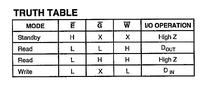
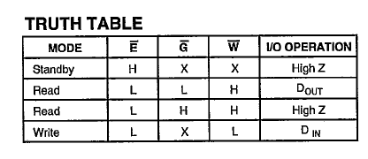
This will work, because when !OE and !WE are both active, SRAM is in write mode, according to datasheet:
Doing the same trick on 29f040 flash memory does not work. That is becase when both !WE and !OE are active in 29f040 flash, the memory is in unknown state.
So I have two solutions:
1. Create W/!R by inverting R/!W and connect:
- !CE to out from address decoder
- !OE to W/!R
- !WE to R/!W
This works well but need extra logic for generating W/!R (extra output if using CPLD/FPGA for example)
2.
- tie !CE to GND
- tie !OE to out from address decoder (address decoder generates 0 when reading $8000-$FFFF and 1 in any other circumstance)
- tie !R/!W to R/!W
This also works well (and does not need any extra outputs, because we still need to have address decoder, just slightly modified) but writing to any other adress than $8000 still makes the memory to interpret this write cycle. Luckily, 29f040 need special 4 cycle write command to program one byte: 5555H/AAH, 2AAAH/55H, 5555H/A0H, PA/PD and 6 cycle command to erase whole memory, so it would be very improbable to inattentionally overwrite any bytes.
Do you have any other ideas?
If I would like to connect SRAM to 6502, I would just connect:
!CS to some kind of decoder
!OE tied to GND
!WE to R/!W from CPU.
This will work, because when !OE and !WE are both active, SRAM is in write mode, according to datasheet:
Doing the same trick on 29f040 flash memory does not work. That is becase when both !WE and !OE are active in 29f040 flash, the memory is in unknown state.
So I have two solutions:
1. Create W/!R by inverting R/!W and connect:
- !CE to out from address decoder
- !OE to W/!R
- !WE to R/!W
This works well but need extra logic for generating W/!R (extra output if using CPLD/FPGA for example)
2.
- tie !CE to GND
- tie !OE to out from address decoder (address decoder generates 0 when reading $8000-$FFFF and 1 in any other circumstance)
- tie !R/!W to R/!W
This also works well (and does not need any extra outputs, because we still need to have address decoder, just slightly modified) but writing to any other adress than $8000 still makes the memory to interpret this write cycle. Luckily, 29f040 need special 4 cycle write command to program one byte: 5555H/AAH, 2AAAH/55H, 5555H/A0H, PA/PD and 6 cycle command to erase whole memory, so it would be very improbable to inattentionally overwrite any bytes.
Do you have any other ideas?