Hi,
I've just gotten a Famicom that I would like to AV mod. This is the standard HVC-CPU-05 revision. However, I'm unsure about what mod to go for.
I've read through forums all the way back to 2009 and up today and there seem to be a wide range of possible solutions, all with their own pros and cons.
The goal for me is to have the cleanest composite signal without jail bars and interference. Mono audio (without buzz'ing) is ok, since I already have multiple other solutions to cover stereo (Like the NT Mini). I've also looked at premade kits like the ones sold here:
- Console5.com -
https://console5.com/store/nes-toploade ... d-kit.html (Based on the original AV Famicom schematics?)
- Otakus-store -
http://www.otakus-store.net/en/modding- ... cable.html (No idea what this design this is based on... Claim to be free from jail bars?)
- Retrofixes.com -
https://store.retrofixes.com/products/o ... pgrade-kit (Single transistor mod with a few extra caps for audio filtering?)
All suggestions are welcome.
-Eicar
I also wonder about this. I have done 2 AV mods where I removed the PPU and wrapped it in copper tape, replaced caps, added extra bypass caps all over the place, used all thin coax wires, etc., and 1 of those famicoms still had very slight jailbars. I wasn't sure what else to try.
I have had GREAT experience with using a single 1/8" TRRS jack out the side of the famicom, then the appropriate AV cable. It is a very clean minimally-destructive way to get AV out of the famicom. Beware though that there are 2 slightly different lengths of TRRS and it does matter.
Eicar wrote:
All suggestions are welcome.
I suggest not modding your Famicom at all. Try an AVS instead.
Ben Boldt wrote:
I also wonder about this. I have done 2 AV mods where I removed the PPU and wrapped it in copper tape, replaced caps, added extra bypass caps all over the place, used all thin coax wires, etc., and 1 of those famicoms still had very slight jailbars. I wasn't sure what else to try.
I did a
very simple mod and ended up with
only very slight jailbars.

For an example of how slight:
here's a video.
I kinda feel like jailbars on a Famicom AV mod are mostly down to luck, some devices are just worse than others no matter what you do. I'm uncertain whether desoldering the PPU to apply copper tape is helpful enough to justify doing.
(Edit: I forgot to mention I also put a bypass capacitor across the PPU power source. It's a very non-invasive addition that I think is worth trying before considering taking the whole PPU out.)
Ben Boldt wrote:
I have had GREAT experience with using a single 1/8" TRRS jack out the side of the famicom, then the appropriate AV cable. It is a very clean minimally-destructive way to get AV out of the famicom. Beware though that there are 2 slightly different lengths of TRRS and it does matter.
TRRS is an interesting way to connect. I just used 2 x RCA, myself.
rainwarrior wrote:
The copper tape and the rest of that seems like superstition to me.
Shielding is sort of unpredictable and hit & miss, but it is a real thing. It makes more of a difference the higher frequency and longer lengths that you are dealing with. To your point, composite video across 5 inches of unshielded wire (~1 inch of which is inside the PPU chip) is probably on the threshold where it starts to matter.
One instance where I know that shielding made a huge difference was with my Sega Genesis SCART cable. The cable I bought was not shielded at all and it had pretty nasty jailbars and ghosts on the screen. I chopped off both ends, and also chopped both ends off of a VGA cable. I then soldered the SCART ends onto the VGA cable, and the difference was amazing. I hoard VGA cables from recycle bins ever since. It also slightly improved my SNES SCART experience when I did this.
Sorry about the way I said that. Yes I didn't mean that shielding isn't a thing, I just don't think it really helps with the Famicom AV mod, from all the accounts I've heard over the years. Every account I'd heard of it was either that they ended up trying it but it didn't fix the jailbars, or they had done it anyway without trying something easier first so there was no comparison, and I'd also heard of several people (myself included) who don't have much of a jailbar problem without doing it.
Though, if you did try it both ways and found it made a noticeable difference, that would be good to know your experience. I haven't tried it myself ('cause I got jailbar-lucky), I'm just going by what others have said about it, and desoldering the PPU is a lot of work and risk of failure if it's not really going to help.
rainwarrior wrote:
I did a
very simple mod and ended up with
only very slight jailbars.
For an example of how slight:
here's a video.
I kinda feel like jailbars on a Famicom AV mod are mostly down to luck, some devices are just worse than others no matter what you do. Desoldering the PPU to apply copper tape seems like superstition to me.
(Edit: I forgot to mention I also put a bypass capacitor across the PPU power source. It's a very non-invasive addition that I think is worth trying before considering taking the whole PPU out.)
TRRS is an interesting way to connect. I just used 2 x RCA, myself.
Thanks! I will probably start with the same schematics and take it from there. Btw, did you use the 2sa937 transistor or something else? Also, did you use an electrolytic capacitor, or a ceramic one for the PPU VCC/GND? Do you remember the capacity?
I'll post the result later. I'm still waiting for some parts in the mail

** Update: I Just found a pile of 2sa1015... They are also PNP transistors so I guess they can be used as a replacement for the 2sa937? **
-Eicar
I used a
2N3906, which I believe is an extremely common part, but I don't know transistor part numbers intimately so I can't help suggest substitutes. Check the datasheets maybe.
I can't remember what capacitor I used, it was several years ago now. Might have actually been a large ceramic I had on hand, or possibly tantalum. I think I was avoiding electrolytic (personal paranoia?), but I assume polarized is fine for this application.
Edit: Ben Boldt suggests that ceramic is the way to go, below.Sorry, I'm not much help for the details. I didn't design the circuit I was just following a recipe (+ the bypass cap which just seemed like something worth trying). Maybe Ben Boldt or someone a bit more versed than me in this topic could comment about substitutions. All I have to offer is my own anecdote of one successful mod, and what I've heard reported by others.
I used to be a HUGE fan of tantalums but got scared of them lately. If they get reverse voltage at all, it can be doom for the cap. I think tantalum might not be the best choice here, they work their magic best on voltage rails and things that always stay positive. But these days, there are very good and cheaper alternatives to tantalum.
I am not sure about transistor substitutions for video signal. In the site I linked to, it had me remove a transistor and re-use it for this purpose, so that is what I did.
Bypass caps should be ceramic and small in value, recommend 10nF. Anything 1-100nF is OK. The purpose of the bypass cap is to "short out" high frequencies, which means low ESR at high frequency. That is what small ceramics do best. It might be tempting to put a big 100uF electrolytic for this purpose, but bigger isn't better. A big electrolytic won't have any effect at all at high frequency where you need it, really defeating the purpose. Bigger is not better in this case - use ceramic with short leads.
The 2sa1015 appears to be working just fine. I just made a temporary breadboard build just to test it and the image quality on my Sony PVM is actually very nice... I mean this is all looong cable lengths connected to a breadboard. I'm actually very surprised that it looks this good. @Ben: What you say about ceramic caps also makes a lot of sense. I've previously repaired jamma boards and those are usually filled with 104 caps (100nF) all over to filter noise. Those board are also very big and often two boards connected together so noise filtering is also very important. (If anyone is interested you can read more about my repair work on my blog-page:
https://www.retrobits.no/).
However, back to my famicom. I do have jail bars. I've used SMB to test because it has a nice blue background. I'll probably get some time this weekend with my oscilloscope, so then hopefully I will be able to find the source of the problem.
I like to investigate problems first.. I don't do random things and hope for the best.. I've attached a few images if anyone is interested...
-Eicar
I was planning on testing this out too. I have a version 6 PB.
The copper shield can do some help. Also, putting the PPU in a high-quality socket may help too, since it increases the distance from the board traces, which is what the copper shield is protecting the PPU from.
The 2 systems that have AV built in (AV Fami, NES) have inductors in their video path. The NES has 2 - there is one extra in the RF/AV box, probably to help filter out noise picked up from the RF modulator components. The other one in the NES and the AV Famicom are ferrite beads.
The original Famicom does not have an inductor in the video path. I think the top-loader does (have to check again), but with the AV mod, it is bypassed.
I find it interesting that all these circuit leave it out, or say "not necessary". Who tested that they are not necessary? It would be interesting to see what the frequency is of the jailbars with the o-scope.
As far as the transistor to use, any jellybean PNP will work. It is being used as a buffer.
Hi again!
I've reached the end of round 1 when it comes to researching this. To sum it up, I've NOT been able to find the real source of the problem for the jailbars, however i have been able to remove ALL jailbars from the composite video signal. I would also like to mention that I almost have zero knowledge on analogue video signals. I've always lived my life on the digital side, so all this it pretty new to me. I'm just trying to learn as I go along. There's also no better way to learn something than to actually get your hands dirty. If I'm writing something here that's completely wrong, or incorrect then I would very much like to get some feedback. My main motivation here is to learn about analogue electronics and any help is appreciated.
So as someone mentioned earlier, small ceramic caps like 100nF between Vcc and Gnd will remove high frequency noise from the input. Most arcade jamma-boards are saturated with them. I tested multiple ceramic caps between the PPUs VCC and Gnd However, this does not have any impact on the jailbars at all. And to me it also makes sense. Jailbars must be caused by a repeating cycling interference to the signal as it has a very defined and visible footprint on the observed video signal. When I looked at the VCC on the board it struck me that the VCC looked "polluted" and also to some degree unstable. VCC would oscillate in the 4,7v-5,2v range depending on where I looked at the signal. The frequency was not clearly visible. My theory is that aging components on the board have started to drain more current over the years due to corrosion and leaking caps and that they are causing a voltage drop+interference to the VCC/Gnd planes. So, my next step then was to try to stabilize the VCC on the board. I first looked at the big 1000uF cap by the 7805 voltage regulator on the PSU. However, after removing and testing it I found that there was nothing wrong with it. It still had the 1000uF capacitance. Next, I tried to solder another 1000uF parallel to the first one, however that also didn't have any impact on the situation. Since I have the VCC and GND from the PPU out on my breadboard I then started to test different electrolytic capacitors to see if it had an impact on the jailbars. And it turned out it did! Starting with a 22uF it turned out to weaken the jailbars slightly. I then started to increase the capacitance and when I reached 100uF all the jailbars were completely gone. And I mean COMPLETELY gone! I also tried a 1000uF however, it didn't make it any better. After all it was more or less perfect already. The VCC looked better on my oscilloscope now as well. The oscillating variance was gone and there was only some brief noise/jitter left. I then played SMB for some time just to see how it looked. I noticed that sometimes like every 20-30 seconds I could see some white scanlines on random locations. If this is caused by ground noise going into the the EXT pins on PPU or if it's caused by noise on the VCC i don't know. However, when I applied a 100nF ceramic cap between the PPUs VCC and GND then the problem dissappeared. I played SMB for about one hour without any glitches so I'm quite happy with the result.
I also tried all the other "solutions" mentioned elsewhere with lifting the PPUs video pin. I actually went as far as removing the PPU completely using my vacuum de-soldering station. However, this did NOT have any impact on the jailbars at all. I also socketed the PPU, however I later reverted this at it would interfere with the eject button on the console. There's basically not enough room to socket the PPU. The grounded copper tape approach also didn't do anything at all so I never glued it on my PPU.
I also tried different video amp designs on my breadboard but I ended up with the amp design from Console5. This proved to give an excellent image on my PVM. It also has a simple high-pass filter on the output for removing the DC offset skew. Some designs also has a 560pF low-pass filter which I think will remove noise above 2,4Mhz or so. However, my video was already noise free so I didn't add it. I guess the my PVM and normal CRT TV already has some filtering builtin as well. (Isn't 2,4Mhz low-pass filter a bit too low anyway??)
I've added a few images here. However, the result looks better in real-life..
All feedback is appreciated!
-Eicar
This is probably one of the most useful/detailed posts I've seen talking about solving the actual problem on an AV-modded Famicom. I actually appreciate it, even though I choose not to mod consoles (though I may make an exception for one particular system I have, keep reading).
I have lots of questions. I'll start with these. You said what fixed the jailbar problem for you was:
1. Adding a 100uF electrolytic capacitor...
1a. ...which is JWCO brand, and spec'd at 16V, as I could tell from the picture...
1b. Between what and what? It isn't clear exactly from your story, you just say you had PPU VCC and GND hooked up to a breadboard and then kinda "magic!"
1c. Since electrolytic caps are polar, what did you connect the positive and negative legs to?
2. Adding a 100nF ceramic disc capacitor between PPU VCC and GND...
2a. Is this the cap labelled 104 in your photo? (It's the only ceramic I see in the photo)
2b. What voltage?
3. What is the JWCO brand capacitor depicted in your photo on the far left of the board? Is it related to the jailbar problem? If not, ignore. If so:
3a. What is it wired/connected to?
3b. What are its specs?
3c. Since electrolytic caps are polar, what did you connect the positive and negative legs to?
More things, saving the best for last:
4. For your electrolytic cap(s) you used JWCO (Jiaweicheng Electronic Co. Ltd / 佳维诚电子有限公司) brand caps, from Shenzhen, Guangdong, China. I've used these caps myself with general success -- they're inexpensive, easy to get, and "get the job done" -- but the badcaps.net forum and
eevblog forum both consider them to be "best-effort" and not long lasting. If you plan on keeping your modded Famicom in good condition, I'd suggest picking another cap brand (Rubycon, Nichicon, Panasonic, ELNA). They're quite a bit more expensive, but you can find them on eBay from reputable places (if you want eBay seller names within the US that are worthwhile, let me know, as I've bought from a couple and would be happy to give you links to them).
5. Did you have jailbar problems with the Famicom
before you did your AV mod, or only after? I think this piece of information is crucial. We do know that the jailbar problem can plague both RF and non-RF Famicoms (I have an actual real/non-modded AV Famicom myself, but also have a top-loader NES (RF)).
Why I ask what I did about #5: now if only people could figure out how to solve this problem in this particular manner for the NES top-loader, which is mostly RF-only and notorious for having some of the worst jailbars you've ever seen. I own one (I bought it shortly after it came out, so roughly early 1994), yet it's always been this way. I don't want to hijack this thread for the NES top-loader -- we have several threads on that system/subject already, but all of them are pretty much "black magic" dust heaps of generally vague and not-very-helpful information. The only thing
we do know for sure is that some SUPER rare top-loaders (very late-gen) actually had
a completely redesigned circuit board (see pictures in linked thread; the right PCB is the redesigned one): one was still RF, the other used a multi-out jack similar to the real AV Famicom (not modded) and thus was composite, and both completely rectified the problem. The rare ones were supposedly only repaired models (back when you could send your products into Nintendo for repair + serviced + sent back to you), not actually sold-on-the-shelf models.
Hi,
That was alot of questions. I'll try my best to answer...
1. Yes! I put it between PPU VCC (pin 40) and GND (pin 20). Minus on CAP goes to GND like in a normal bypass cap setup.
1a. Yes, I ordered a huge pack from china with different values a while back. I'm guessing they're not the best electrolytic caps based on the price and they might dry out over the years. I can replace them again if needed.
1b. I soldered two wires from PPU pin 40 and pin 20 to my breadboard. It was then easy to hot-swap different bypass caps on the breadboard to see the results live.
1c. + goes to PPU pin 40 (VCC), and - to PPU pin 20 (GND)
2. Yes, between the same pins as above
2a. Yes, it's a normal 104 ceramic disc (100nF). You see it right under the PPU between pin 20 and 40. I used shrink plastic to cover the legs. I love shrink plastic
2b. I have no idea. These are no-name ones. Normally 104s should survive 50V.
3.
Ok, let's clear up a few things here. After I did the breadboard testing I also discovered that the location of the 100uF didn't matter that much. So instead of soldering it directly between pin 20 and 40 I ended up soldering it between VCC and GND on the left side of the PCB. This is still quite close to the PPU. Since there was a nice place further up to the right side of the board as well I also put a second 100uF there. This didn't have any impact on the image in anyway. You must remember that these bypass caps are only there for flattening the DC voltage on the board. However, electrolytic caps will not filter high frequency jitter. For that you need lower values ceramic disc capacitors (like the 0.1uF = 100nF). The discs should also be placed as close to the chips VCC/GND pins as posible to make it as efficient as possible. The larger electrolytics are just "buffers" that will stabilize the VCC across the pcb. I added two on the PCB. One would have worked just as fine. The red and black cable on the left side of the PCB (VCC+GND) goes to the actual video amp together with PPU video out pin 21.
(I ended up lifting the leg from the board since I had already taken it out. However, it didn't effect the jailbars if it was lifted or not. I tested both.) This circuit is "hidden" in the lower left part of the case. You can can see some resistors etc. there it you look closely. The final video out then goes along the joystick cable on the left side and all the way out the back. I also hooked up audio out from pin 46. I sent this through a 1kOhm resistor and a 22uF cap to remove any DC voltage from the output. This also works as a high-pass filter.
4. I'm not going to argue with you here. I'm well aware that these caps are probably not the best. I always measure the capacitance of the caps before I use them. If they are far from the labeled value then they go to the recycle bin. How long they will live I also don't know. If you have URLs to good quality electrolytic caps with good prices then by all means I would like to know.
5. I live in the PAL region of the world. Even though my PAL TV can deal with NTSC composite signals it's unable to tune in on Japanese RF frequencies. This also means that I have no idea if the jailbars are present on the RF part of the signal. I've only seen the composite signal via my own av amp. This is the circuit I used for my mod:
https://console5.com/wiki/File:NES_Topl ... ematic.pngI will probably try to get hold of more famicoms. Even broken ones, just pcbs or the once in bad shape just to research this further. If you know anywhere I can buy old famicoms in bulk for a good price then please let me know. Buying one by one from ebay gets expensive quickly due to the shipping cost. If I could by 4-6 in one batch from somewhere it would be great!
I hope I was able to give you some satisfying answers.
-Eicar
Is your TV
"cable-ready" in the sense that it has a mode for various countries' analog cable band plans? If so, I've made
another topic about receiving RF signals on a non-Japanese TV.
PAL TVs that also accept baseband NTSC usually cannot tune to any 6 MHz RF-modulated channel at all, no matter what frequency band the channel is in.
Yes, I believe this is true for my PAL TV as well.
And I also don't care that much about RF either. Composite is better on all areas anyway.
-Eicar
That's good you got it looking good. Everyone seems to find a solution that "works for them". Unfortunately, what works for you, might not for someone else. What is the solution that works for everyone?
It's best to figure out what is causing it so it can be eliminated. The video signal needs to be seen on an o-scope, preferably running 240p Test Suite so we can get a full screen of one color. This will make it easier to see the interference on the video signal. Also, the 5V line should be looked at for noise. You said you saw the voltage drop?
I'm really surprised no one has bothered to take a deep look into it (other than the Japanese guy Taivatri-
Translated PageI have all 4 systems. I do plan on testing this when I have some time, along with the audio path and a better way to mix in expanded audio.
Adding capacitors to the 5V line is just adding more bypassing for high frequency noise. You usually see capacitors near every logic IC on any electronic device for this purpose. The cap should be placed as close as possible to the IC. That's what you are seeing on the JAMMA boards, because there are a ton of logic ICs on them. These are usually tantalum or dipped ceramic caps. Sometimes a tantalum and ceramic in parallel is even better. Really depends on the noise on the 5V and the frequency of it. The most important thing is that they are placed as close to the IC power pin as possible, with as short leads as possible.
Also, the AV circuit works as so - the 220uF cap in combination with the 75 ohm in the TV form a high pass filter to remove the DC component (bias) from the signal. 220uF is probably the lowest I would go. You can increase the capacitance but wouldn't make much difference to the signal. The transistor configuration is a buffer that is used to drive the video signal. The circuit used is derived from the one in the AV Famicom.
rainwarrior wrote:
desoldering the PPU is a lot of work and risk of failure if it's not really going to help.
I 100% agree -- Removing the PPU has a high risk of damaging the circuit board, ripping out barrels. It should not be attempted unless necessary. I have no data to support wrapping the PPU in foil makes any measurable difference at all. In fact, the board itself probably has a +5V and/or ground plane under the chip anyway, which would already serve this purpose.
However, all of the AV mods I have seen require disconnecting one of the pins of the PPU from the circuit board. I think if a person is experienced with desoldering DIPs, it might be the better route to remove the PPU instead of cutting a pin. In which case, as long as you have it out, may as well be superstitious and put foil on it.
Ben Boldt wrote:
However, all of the AV mods I have seen require disconnecting one of the pins of the PPU from the circuit board.
I didn't disconnect anything for my mod. What pin are you disconnecting?
rainwarrior wrote:
Ben Boldt wrote:
However, all of the AV mods I have seen require disconnecting one of the pins of the PPU from the circuit board.
I didn't disconnect anything for my mod. What pin are you disconnecting?
Oh wow, really? I found that foreign site with Google Image Search, liked what I saw, and pretty much just followed what it said from there. I disconnected pin 21 VOUT from the PCB, and then built a small circuit up directly off of that pin. I know that I was never actually aware of the reason (or lack thereof) that they disconnected the pin - I had assumed that it was necessary.
I assume some people want to isolate it from the original RF output path. Like desoldering the PPU, I wouldn't recommend it until you've tried the easier stuff.
Does it even connect to more than one place on the board, though? Wouldn't it make more sense to follow it to the next component it connects to and break the circuit there, than do something irreversible like cutting a PPU pin?
The best way to know for sure is to try it, but I am betting it does not make much of a difference. All I know is that there is no way in heck I would have cut the video pin on my PPU. I saw pictures of people doing that and even grinding away the package to get deeper down the pin. I thought that was pretty crazy and moved on without a second thought.
Edit:
Actually I just went back and found that again, they were fixing broken PPU pins that broke when they tried bending them during an AV mod, it was not part of the AV mod itself, thank goodness, because that would have been pretty extreme.
http://nintendoage.com/forum/messagevie ... did=121453

Ultron wrote:
That's good you got it looking good. Everyone seems to find a solution that "works for them". Unfortunately, what works for you, might not for someone else. What is the solution that works for everyone?
It's best to figure out what is causing it so it can be eliminated. The video signal needs to be seen on an o-scope, preferably running 240p Test Suite so we can get a full screen of one color. This will make it easier to see the interference on the video signal. Also, the 5V line should be looked at for noise. You said you saw the voltage drop?
I totally agree with everything you say. I'm not finished with this yet. I've already bought more famicoms to investigate this further. The next one will be a 07 board. This has much bigger VCC and GND planes. It will be interesting to see if this has any impact on the jailbars compared to the 05 pcb. I already tried looking at the video signal using my oscilloscope, however I'm not an expert on using it yet so I wasn't able to get a good lock on the signal. I'm also not sure if it's that important either. After all, in my mod I lifted the video out pin from the pcb, meaning that all interference must come from the PPU VCC, GND or any other PPU pin? Adding a 100uF electrolytic cap between the VCC and GND removes whatever noise from the lines and also removes the jailbars. I also found out that the 100uF cap could be placed on different locations on the PCB and it would still remove the jailbars. The noise must be coming from somewhere else on the board.
Ultron wrote:
Adding capacitors to the 5V line is just adding more bypassing for high frequency noise. You usually see capacitors near every logic IC on any electronic device for this purpose. The cap should be placed as close as possible to the IC. That's what you are seeing on the JAMMA boards, because there are a ton of logic ICs on them. These are usually tantalum or dipped ceramic caps. Sometimes a tantalum and ceramic in parallel is even better. Really depends on the noise on the 5V and the frequency of it. The most important thing is that they are placed as close to the IC power pin as possible, with as short leads as possible.
Yes, as far as I understand when it comes to very high frequency noise that you would filter out with a 0.1uF ceramic cap, then it needs to be very close the logic IC. However, in this case I had to use a 100uF electrolytic cap to filter out the VCC noise. This is not as sensitive when it comes to the distance from the actual chip. I mean I even tested adding this cap to my breadboard... That's about 15-20cm cable length from the PPU pins... and it removed all jailbars. A 0.1uF didn't have ANY impact on the jailbars even when solder directly between the VCC and GND pins. However, this fixed the flickering pixels that sometimes occurred during testing. This is the result of high frequency noise/spikes, and the small ceramic between VCC and GND will take care of that.
Ultron wrote:
Also, the AV circuit works as so - the 220uF cap in combination with the 75 ohm in the TV form a high pass filter to remove the DC component (bias) from the signal. 220uF is probably the lowest I would go. You can increase the capacitance but wouldn't make much difference to the signal. The transistor configuration is a buffer that is used to drive the video signal. The circuit used is derived from the one in the AV Famicom.
Thanks for pointing that out. That makes perfect sense. I was running some simulations and it worked a lot better with the added 75ohm on the TV side
My next step will be to do some frequency analysis of the VCC noise using fast fourier transformations. I want to see what frequencies we are dealing with.
It might be that all of this comes down to poor PCB design in the famicoms. After all, when you look at the NES or the AV famicom you have a lot of shielding and much bigger VCC+GND planes.
I also suspect that ICs as they age can generate more noise than what they did when they were factory new. Maybe the noise margins in the PCB design is just so small that small variations
will have dramatic impact on the video quality. (like jailbars...)
-Eicar
Ben Boldt wrote:
rainwarrior wrote:
desoldering the PPU is a lot of work and risk of failure if it's not really going to help.
I 100% agree -- Removing the PPU has a high risk of damaging the circuit board, ripping out barrels. It should not be attempted unless necessary. I have no data to support wrapping the PPU in foil makes any measurable difference at all. In fact, the board itself probably has a +5V and/or ground plane under the chip anyway, which would already serve this purpose.
However, all of the AV mods I have seen require disconnecting one of the pins of the PPU from the circuit board. I think if a person is experienced with desoldering DIPs, it might be the better route to remove the PPU instead of cutting a pin. In which case, as long as you have it out, may as well be superstitious and put foil on it.
I don't believe in the foil wrapping either. However it might have some impact since it effectively increases the ground plane under the PPU. As you can see from my photos, there's not really a big ground plane under the PPU. Howver, I'm still following my theory regarding VCC noise. Removing and lifting the PPU didn't have any impact on the jailbars. I don't think the kind of video amp circuit matters at all either. The jailbars are already present on the video out pin. There's nothing to do about it at that point. It needs to be solved earlier in the signal chain.
-Eicar
What are the jailbars synchronized to? They stay stationary on the screen. Are they occurring on each PPU /RD transition or each CPU clock transition, etc? Finding the source could lead us to new ideas. For example, if it is PPU /RD, adding a fast CMOS buffer might have potential.
Another potential, which could be easily ruled out depending on how the jailbars are syncing, would be to replace the 74LS373 with a 74HC373 and see what happens. This would have higher impedance inputs and theoretically not be loading the PPU Address/Data pins as much at each transition.
It might also be interesting to take a piece of ferrite and hover it around different parts of the board and see if any particular area affects the jailbars.
Ben Boldt wrote:
What are the jailbars synchronized to? They stay stationary on the screen. Are they occurring on each PPU /RD transition or each CPU clock transition, etc? Finding the source could lead us to new ideas. For example, if it is PPU /RD, adding a fast CMOS buffer might have potential.
Another potential, which could be easily ruled out depending on how the jailbars are syncing, would be to replace the 74LS373 with a 74HC373 and see what happens. This would have higher impedance inputs and theoretically not be loading the PPU Address/Data pins as much at each transition.
It might also be interesting to take a piece of ferrite and hover it around different parts of the board and see if any particular area affects the jailbars.
In the link I posted, the guy said it comes from the pin 25 trace.
You are 100% correct, they are stationary and never change location. Good ideas too!
One thing I noticed with the AV Famicom board is that it looks like it's a 4-layer board. So there would be a VCC and GND plane as the middle 2 layers, with traces on top and bottom. This, I believe, is why they don't have the jailbar issue.
That's great!
I hope the findigs here can ba used to remove jailbars once and forever from the NESes out there and clones!
Keep going! I'll try the LS to HC exchange as soon as I can!!
Fisher wrote:
That's great!
I hope the findigs here can ba used to remove jailbars once and forever from the NESes out there and clones!
Keep going! I'll try the LS to HC exchange as soon as I can!!
Sorry to sound like I knew what I was talking about Fisher, I am not sure an HC will even work there -- I didn't look into voltage thresholds of the PPU, etc. It may require an HCT for example. I just threw it out there as an idea. If you are good at removing chips, I don't think it would hurt anything to try it though. It would be interesting even to rule it out.
Ben Boldt wrote:
What are the jailbars synchronized to? They stay stationary on the screen. Are they occurring on each PPU /RD transition or each CPU clock transition, etc? Finding the source could lead us to new ideas. For example, if it is PPU /RD, adding a fast CMOS buffer might have potential.
Another potential, which could be easily ruled out depending on how the jailbars are syncing, would be to replace the 74LS373 with a 74HC373 and see what happens. This would have higher impedance inputs and theoretically not be loading the PPU Address/Data pins as much at each transition.
It might also be interesting to take a piece of ferrite and hover it around different parts of the board and see if any particular area affects the jailbars.
I have two more famicoms coming my way, so I will be testing this when I get them. I don't want to "un-fix" the famicom I already fixed so I will wait for the once in the mail before I continue my researched.
I took a lot of photos of the jailbars on my first Famicom and so far I can conclude that the jailbars are stationary to the background tiles. There's one jailbar for every 8 pixel bg tile. Since we know that the PPU will fetch the bg tiles every 8 cycles into
the two 16-bit shift registers I'm thinking that this read operation if causing some interference on the buss, or a voltage drop on the VCC line. Someone also mentioned on some forum that the Everdrives are causing more jailbars than official carts. It is also my understanding that the Everdrives consume more power than official carts so that this might explain it. However, this information should be taken with a hugh pile of salt as I havn't been able to confirm any of it yet. It's just speculation on my behalf. I will keep you guys updated when I know more.
-Eicar
Ben Boldt wrote:
I am not sure an HC will even work there
I noticed it's just an idea, and I'm willing to try that as soon as possible.
Also in
this topic seems that this change makes a Powerpak work fine with an RGB modded NES.
A guy named Esrael Neto did some mods on a NES clone and published
here.
Maybe this can give some clues about what to do on other clones and even the NES itself.
Looks like the problem on the clone was interference on the power circuit, with insufficent current arriving on the ICs.
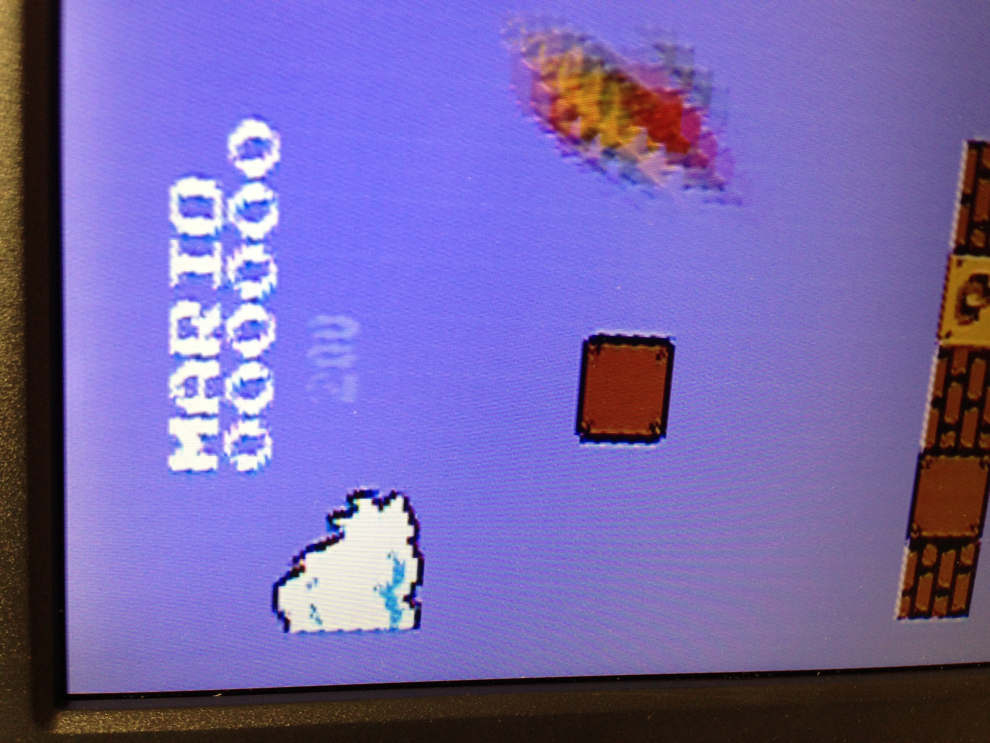
If you were to look at the composite video signal with a scope, and not have a cart handy that could accept the 240p video test ROM, I believe that Super Mario Bros. would be a good one to use because the first 16 scanlines or so are always solid blue during the entire demo loop.
Fisher wrote:
Ben Boldt wrote:
I am not sure an HC will even work there
I noticed it's just an idea, and I'm willing to try that as soon as possible.
Also in
this topic seems that this change makes a Powerpak work fine with an RGB modded NES.
A guy named Esrael Neto did some mods on a NES clone and published
here.
Maybe this can give some clues about what to do on other clones and even the NES itself.
Looks like the problem on the clone was interference on the power circuit, with insufficent current arriving on the ICs.
Okay, sounds good. I ordered some 74HCT373N from China. It will be a while to get here but I will lend a hand if/when needed.
Well, I socketed the IC of my clone and got the same results with an LS part, with an HC part and without the latch.
I just couldn't get good enough pictures.

In fact, I can see no jailbars on the pictures I've got.

Maybe if I try to get the images with a capture card later?
So probably it's not the latch.
Let's see how your tests go.
I'll test other games to see if the HC part does make some games behave different graphically.
Ben Boldt wrote:
If you were to look at the composite video signal with a scope, and not have a cart handy that could accept the 240p video test ROM, I believe that Super Mario Bros. would be a good one to use because the first 16 scanlines or so are always solid blue during the entire demo loop.
Fisher wrote:
Ben Boldt wrote:
I am not sure an HC will even work there
I noticed it's just an idea, and I'm willing to try that as soon as possible.
Also in
this topic seems that this change makes a Powerpak work fine with an RGB modded NES.
A guy named Esrael Neto did some mods on a NES clone and published
here.
Maybe this can give some clues about what to do on other clones and even the NES itself.
Looks like the problem on the clone was interference on the power circuit, with insufficent current arriving on the ICs.
Okay, sounds good. I ordered some 74HCT373N from China. It will be a while to get here but I will lend a hand if/when needed.
Hey bud,
Digikey is in your backyard. They are in MN. -
https://www.digikey.com/product-detail/ ... -ND/277262I order from them all the time.
Hope to have time this weekend.
I would really like to get this on the o-scope.
I have my top-loader NESRGB modded. But the board will still output the PPU composite video. I'm curious if the jailbars are seen there, too.
Ultron wrote:
Hey bud,
Digikey is in your backyard. They are in MN. -
https://www.digikey.com/product-detail/ ... -ND/277262I order from them all the time.
Yes I know!
But the shipping still costs more than the parts for stuff like this.

Fisher wrote:
Well, I socketed the IC of my clone and got the same results with an LS part, with an HC part and without the latch.
I just couldn't get good enough pictures.
In fact, I can see no jailbars on the pictures I've got.
Maybe if I try to get the images with a capture card later?
So probably it's not the latch.
Let's see how your tests go.
I'll test other games to see if the HC part does make some games behave different graphically.
Thanks for trying Fisher. Now we know. I will try it if I am able to find a way to precisely measure the jailbars.
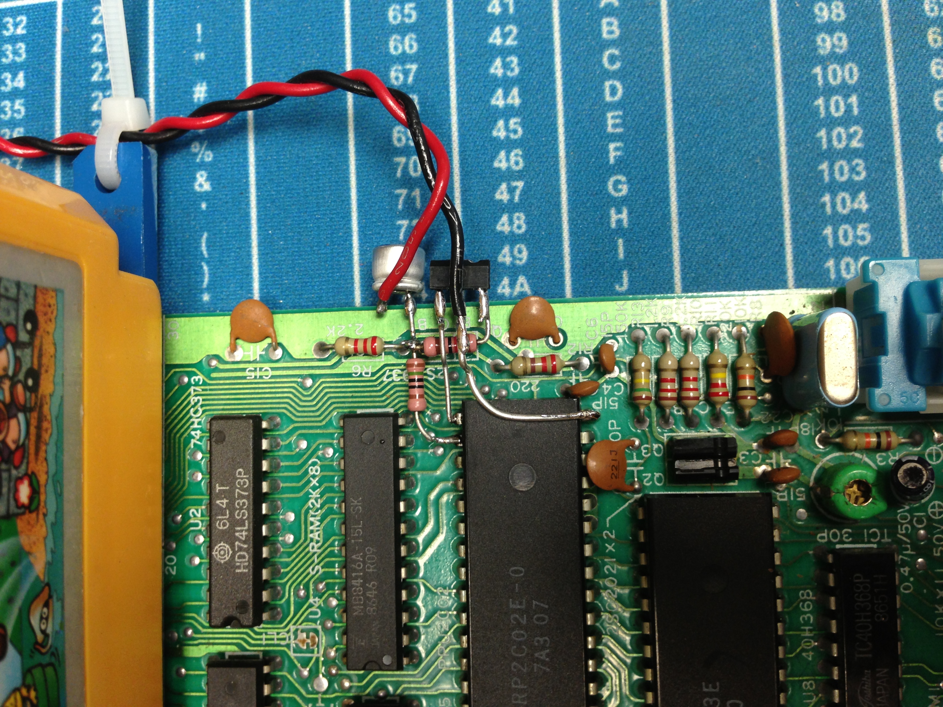
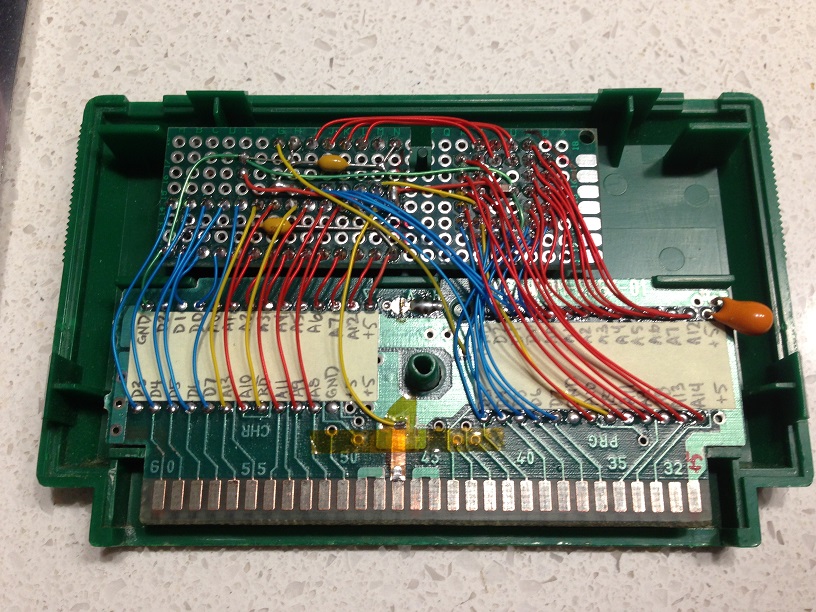
I finally got around to working on this today. I got very lucky (in this case) and found a Famicom with very bad jailbars. Here is the AV mod that I did (video only, no cut traces, no cut pins, no copper foil, etc, only the parts shown):
Attachment:
 av_mod.JPG [ 2.73 MiB | Viewed 3902 times ]
Here are the jailbars with this mod:
Attachment:
 no_cap.JPG [ 2.58 MiB | Viewed 3902 times ]
By adding a 47 uF Tantalum capacitor from pin 22 to GND, it makes an incredible improvement:
Attachment:
 with_tantalum.JPG [ 3.49 MiB | Viewed 3902 times ]
Code:
(GND)
PPU.20 -----------+---------------------------------+
| | |
| | V (c) +----O } Composite
| PPU.21 --|< PNP (Reused the 2SA937) } Video
| | \ (e) 33uF +----O }
--- Magic | 100 Electrolytic |
--- Capacitor +-------/\/\/----+------|(--------+
| |
| (/RST) 150 |
PPU.22 -------------------/\/\/----+
I don't have any particular reason to think my values are any better worse than other mods, this is just the way that I have been doing it in the past. I notice now that my AV mod uses PPU pin 22 (/RST) as the pull-up rail. It seems to me that might be a digital signal and not really a 5V rail, that's interesting, I wonder why it is like that?? I should try using a true 5V, and also tweaking the resistors to be like other mods that are out there.
I tried various "magic" capacitors. I notice these capacitors are good, I can't tell any of them better or worse than each other:
- 47uF 35V Tantalum
- 15uF 35V Tantalum
- 6.8uF 35V Tantalum
- 4.7uF 35V Tantalum
These caps are
almost as good as the tantalums above, almost undetectable difference:
- 10uF 100V Electrolytic (might be a low ESR cap, doubtful but not sure)
- 3.3uF 35V Tantalum
- 2.2uF 35V Tantalum
These caps are are definitely NOT AS GOOD as the ones listed above:
- 1uF 35V Tantalum
- 100uF 16V Tantalum
- 1uF 100V electrolytic
- 100uF 35V electrolytic
- 22uF 16V X7R ceramic (much to my surprise, I suspected this would be a winner)
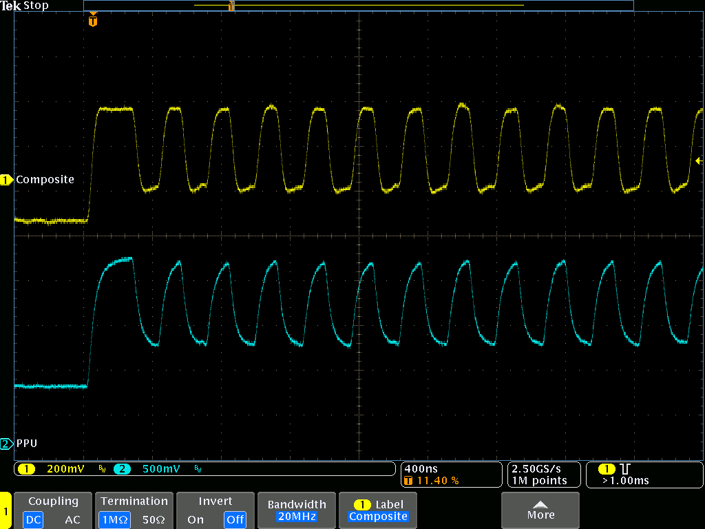
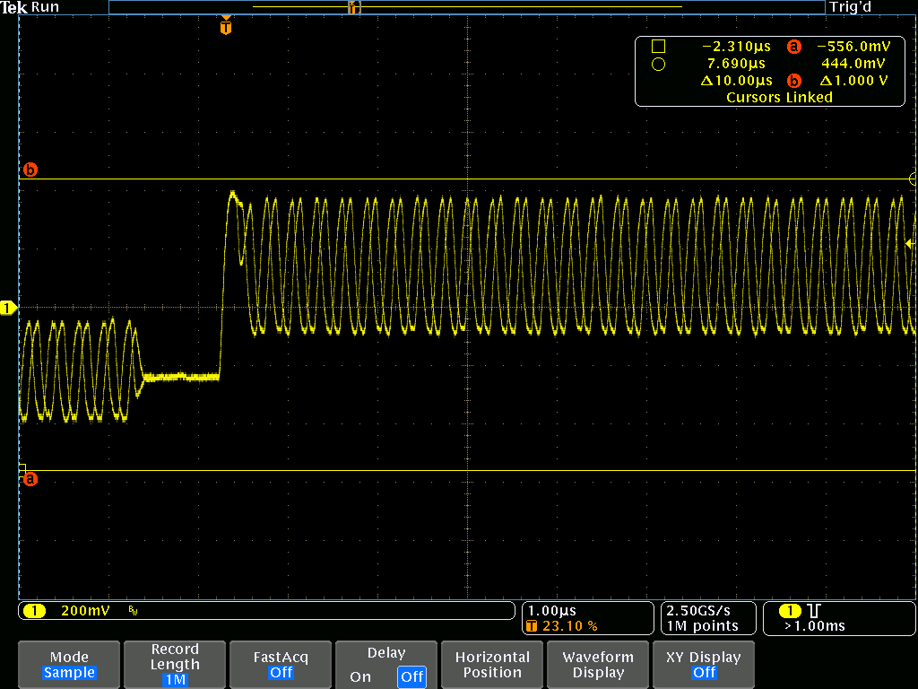
Referring to the oscilloscope, the jailbars should be measurable. Triggering on the first scanline, showing just the first few tiles, running Super Mario Bros. 1 demo (solid sky blue):
Attachment:
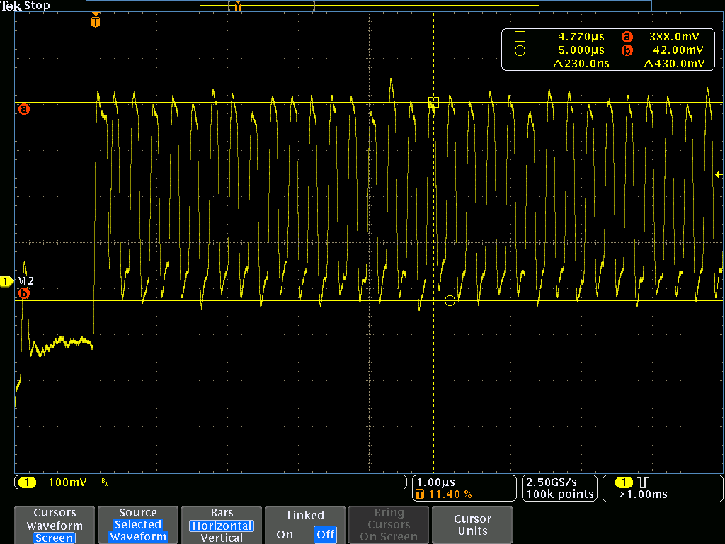 tek00090.png [ 37.47 KiB | Viewed 3902 times ]
With tantalum:
Attachment:
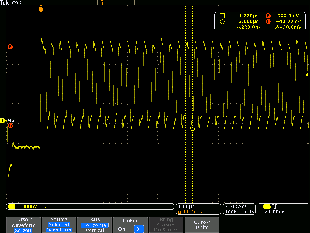 tek00089.png [ 35.8 KiB | Viewed 3902 times ]
I think that if it was perfect, all of the peaks would line up, so I can try experiments and measure the effects now. Also, when viewed in motion with the oscilloscope, the jailbar one has much more variation to it.
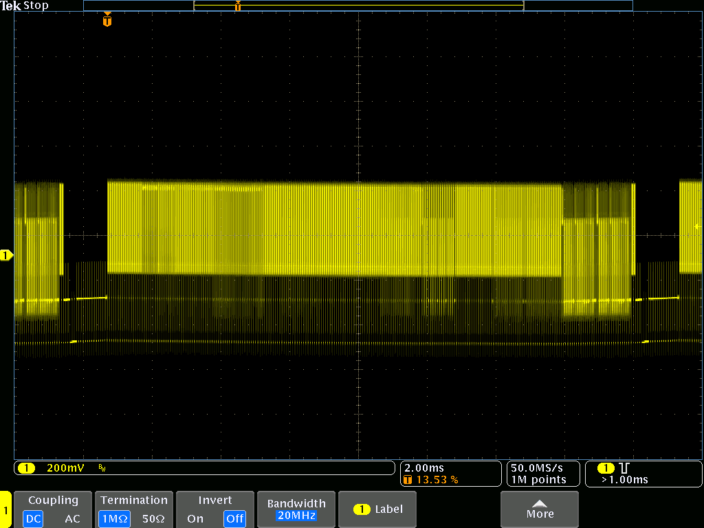
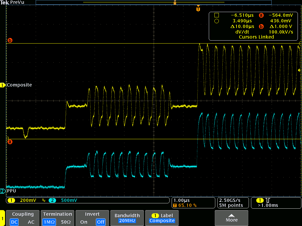
Playing with the 33uF cap (this cap is intended to remove DC bias):
Full frame with 33uF 16V electrolytic:
Attachment:
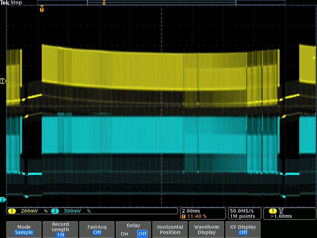 tek00093.png [ 88.61 KiB | Viewed 3890 times ]
Full frame with 100uF 35V electrolytic:
Attachment:
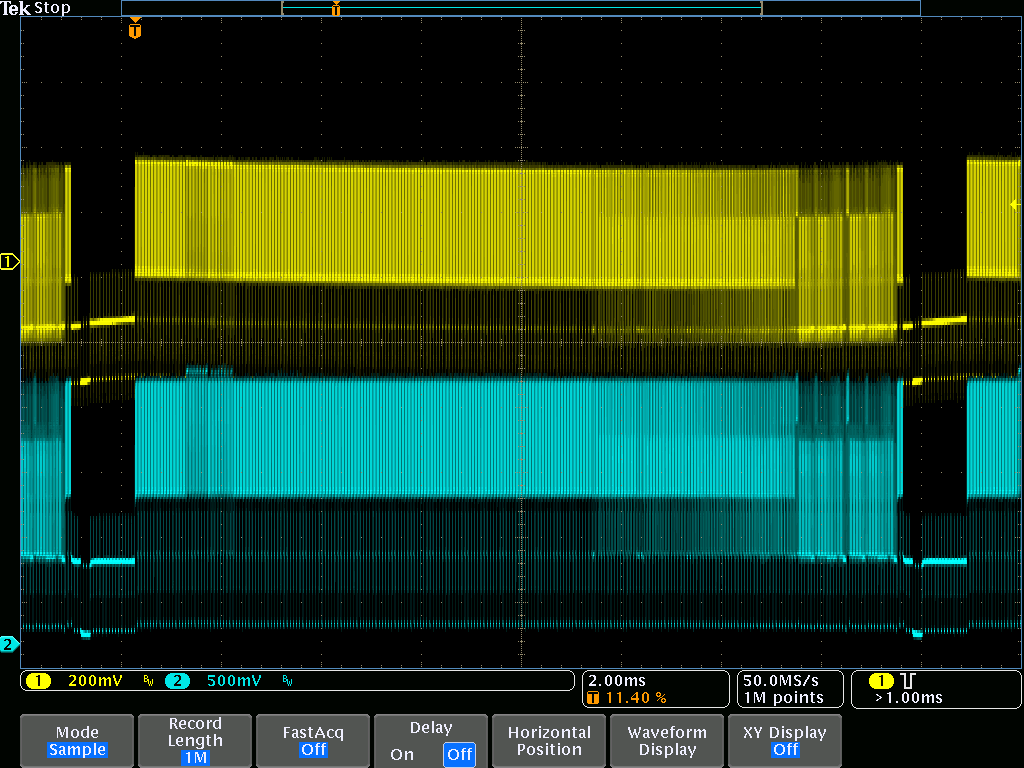 tek00094.png [ 88.45 KiB | Viewed 3890 times ]
Blue = directly from PPU, base of transistor. Notice it is all positive.
Yellow = Composite signal. Notice it is centered positive and negative (i.e. DC bias has been removed)
You can see here that the 33uF creates a quite slanty signal, especially the v-blank, whereas the 100uF seems to be a better choice. My monitor shows no visible difference between 33uF and 100uF. No more or less jailbars, no sharper or fuzzier or anything. I tried adding some ceramic and tantalum in parallel with this 100uF to see if there was any effect to the sharpness but found none.
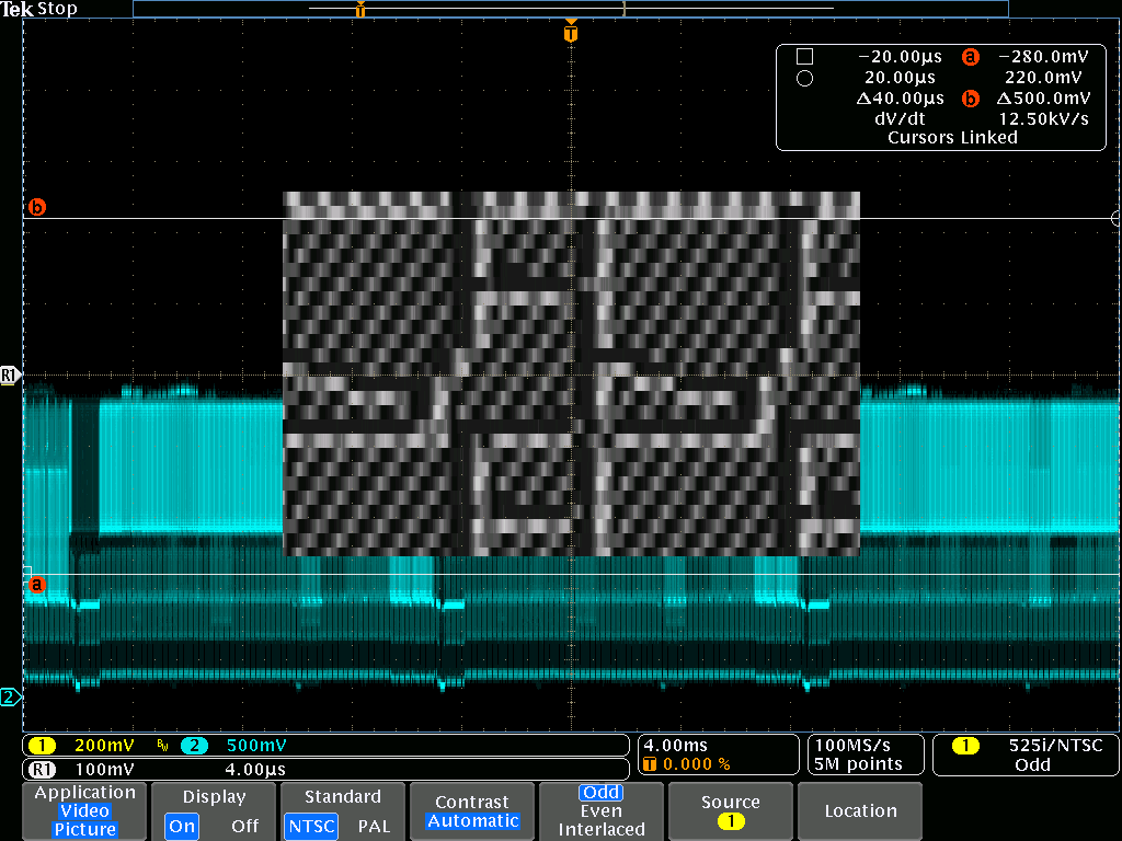
Edit:
Does anyone here know much about composite signals? I thought it was supposed to be a 1 Volt signal and this is only 0.78V: (Showing V-Blank here)
Attachment:
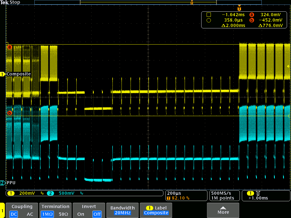 tek00003.png [ 89.97 KiB | Viewed 3883 times ]
Also, some distortion comparing before-and-after the transistor, not sure what this means (Showing first scanline here):
Attachment:
 tek00001.png [ 31.43 KiB | Viewed 3883 times ]
I am wondering if it might be better to use an op-amp here instead of a transistor.
Nice measurements! Though I don't see jailbars in the video signal measured on the o-scope. I'm not sure how to bring them out.
Pixel frequency should be ~5.368MHz. Which is ~186.29 ns period.
Your composite signal with the 30uF shows field tilt. That capacitor should be at least 200uF. Here's a good tech note on field tilt.
https://pdfserv.maximintegrated.com/en/an/AN3768.pdfComposite out of the PPU should be 2V. Then when T'ed off the TV connection, should be 1V. Problem here is, the PNP transistor in an emitter follower configuration has a gain of a little less than 1. I'm thinking that's why it's a little low. Though, from the wiki, it looks like it isn't outputting a 2V composite signal.
https://wiki.nesdev.com/w/index.php/NTSC_videoThanks for doing this!!
Ben Boldt wrote:
Does anyone here know much about composite signals? I thought it was supposed to be a 1 Volt signal and this is only 0.78V: (Showing V-Blank here)
I know more than is healthy :p
But, yes, it's supposed to be approximately 1Vpp, from sync tip to full white (and sync tip to fully saturated yellow is 1.3V). The NES is really rather noncompliant though; see my
measurements on the wiki.
Quote:
I am wondering if it might be better to use an op-amp here instead of a transistor.
Op-amps have tremendously lower gain-bandwidth. You should be able to use a series of emitter-followers to get a perfectly lovely result.
The NES/FC have just the first PNP-based emitter-follower already on the board; what happens after it enters the RF modulator is a question with multiple answers. One of the RF modulators has
a NPN-based emitter-follower on the baseband NTSC output.
lidnariq wrote:
I know more than is healthy :p
Yay!!
lidnariq wrote:
But, yes, it's supposed to be approximately 1Vpp, from sync tip to full white (and sync tip to fully saturated yellow is 1.3V). The NES is really rather noncompliant though; see my
measurements on the wiki.
Interesting, so since there is no white or yellow in the SMB1 demo, I should expect this lower voltage? I suppose I should get the 240p Test Suite running on a cart for this.
lidnariq wrote:
Quote:
I am wondering if it might be better to use an op-amp here instead of a transistor.
Op-amps have tremendously lower gain-bandwidth. You should be able to use a series of emitter-followers to get a perfectly lovely result. The NES/FC have just the first PNP-based emitter-follower already on the board; what happens after it enters the RF modulator is a question with multiple answers. One of the RF modulators has
a NPN-based emitter-follower on the baseband NTSC output.
I was looking at the MAX4390 op-amp, it seems to be intended for this purpose. Though, I never imagined that a single SOT-23 part could cost several dollars! Wow. Do you have any emitter-follower ideas or an example I could try to build? Should I try to copy the circuit from the RF modulator you linked to? I am sort of clueless where to start. Would love to come up with a solid, semi-simple solution for the DIYers out there.
I guess my original intention was to find out where the jailbars are coming from and how to make them the least visible. Improving the video signal might make them MORE apparent! lol
Anyway, I think I can keep poking at it for now. The bad jailbars at first seem like each 4 pixels. When I put on the "magic cap", the very slight jailbars that remain are wider, seems like 8, possibly suggesting an additional source elsewhere.
Jailbars always seem to be from coupling with some of the various digital signals nearby - PPU A13 (4 pixels each on/off) and PPU /RD (1 pixel each on/off) seem to be common culprits. Slower=wider patterns must be something of PPU A0 through PPU A11 - they'll be very heavily dependent on what exactly is being drawn. Depending on context, PPU A12 might look like PPU A13, or be offscreen; PPU AD0-AD7 will change every pixel but won't be predictable.
In the Famicom, PPU /RESET is just tied to +5V, so that's why it seems to work as a bypass point.
Ben Boldt wrote:
Interesting, so since there is no white or yellow in the SMB1 demo, I should expect this lower voltage? I suppose I should get the 240p Test Suite running on a cart for this.
Yeah, you won't see full range of voltage without full range of picture brightness.
NTSC yellow is just particularly high chrominance magnitude. NES yellow-ish isn't any different than any other color in the same horizontal row of the palette.
Ben Boldt wrote:
Do you have any emitter-follower ideas or an example I could try to build?
I'd consider trying the Vs. System 3-stage emitter follower schematic. My two NESes haven't shown any jailbars so I haven't pursued this rabbit hole myself.
lidnariq wrote:
Jailbars always seem to be from coupling with some of the various digital signals nearby - PPU A13 (4 pixels each on/off) and PPU /RD (1 pixel each on/off) seem to be common culprits. Slower=wider patterns must be something of PPU A0 through PPU A11 - they'll be very heavily dependent on what exactly is being drawn. Depending on context, PPU A12 might look like PPU A13, or be offscreen; PPU AD0-AD7 will change every pixel but won't be predictable.
In the Famicom, PPU /RESET is just tied to +5V, so that's why it seems to work as a bypass point.
Ben Boldt wrote:
Interesting, so since there is no white or yellow in the SMB1 demo, I should expect this lower voltage? I suppose I should get the 240p Test Suite running on a cart for this.
Yeah, you won't see full range of voltage without full range of picture brightness.
NTSC yellow is just particularly high chrominance magnitude. NES yellow-ish isn't any different than any other color in the same horizontal row of the palette.
Ben Boldt wrote:
Do you have any emitter-follower ideas or an example I could try to build?
I'd consider trying the Vs. System 3-stage emitter follower schematic. My two NESes haven't shown any jailbars so I haven't pursued this rabbit hole myself.
Okay, I will keep it in mind. It looks like the Vs. System uses RGB + Sync, are you saying we should consider trying one of the 3 color channels for composite on the Famicom?
I changed to a 220uF electrolytic to reduce the field tilt, here is the result:
Attachment:
 tek00006.png [ 58.77 KiB | Viewed 3745 times ]
Ben Boldt wrote:
It looks like the Vs. System uses RGB + Sync, are you saying we should consider trying one of the 3 color channels for composite on the Famicom?
It's where I'd start, I guess? An emitter follower is a voltage buffer, producing the same voltage on the output as the input, plus or minus one diode drop depending on PNP/NPN. Given matched transistors (level of matching discretionary), a PNP and NPN stage will balance out, removing any net DC bias.
Each stage will effectively decrease the output impedance of the previous stage by the β=h
FE of the transistor.
There's also the reverse-engineered schematics from Electronix Corp-
RF modulator and
mainboard - which also show a different PNP+NPN stage from the one I saw in the previous link.
Ben Boldt wrote:
I was looking at the MAX4390 op-amp, it seems to be intended for this purpose. Though, I never imagined that a single SOT-23 part could cost several dollars! Wow. Do you have any emitter-follower ideas or an example I could try to build? Should I try to copy the circuit from the RF modulator you linked to? I am sort of clueless where to start. Would love to come up with a solid, semi-simple solution for the DIYers out there.
I guess my original intention was to find out where the jailbars are coming from and how to make them the least visible. Improving the video signal might make them MORE apparent! lol
Anyway, I think I can keep poking at it for now. The bad jailbars at first seem like each 4 pixels. When I put on the "magic cap", the very slight jailbars that remain are wider, seems like 8, possibly suggesting an additional source elsewhere.
The MAX4389/4390 would work well, but it is pricey. High speed op amps get high in price, and an emitter follower will work fine here.
The AV Famicom and NES include a ferrite bead, FC2 in the video path. This is very often (always) omitted from AV mods. Ferrite beads provide high frequency noise suppression. Problem is, there are no labels on the bead and anything in the NES schematic. It might be worth it to borrow one from a NES or AV Famicom for testing. I attached diagram of the AV Famicom Video Amp (references are arbitrary).
Attachment:
File comment: AV Famicom Video
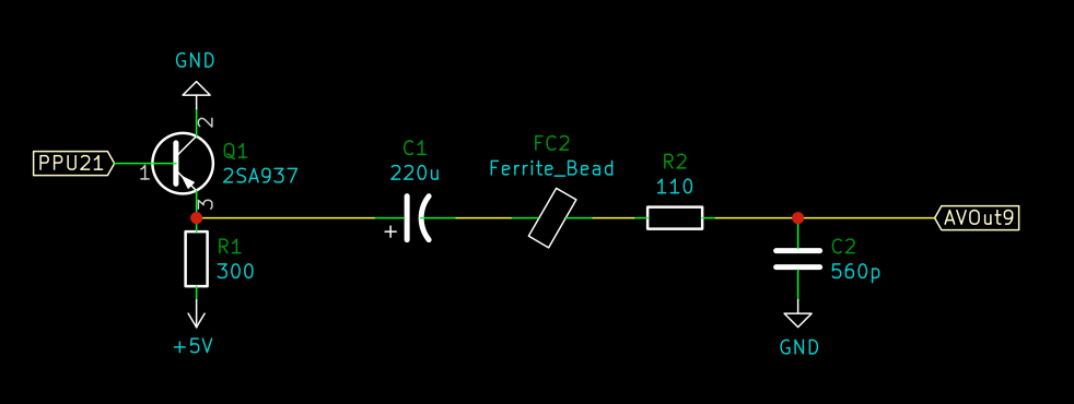 AV Fami Video.png [ 41.08 KiB | Viewed 3620 times ]
For whatever it's worth, the ferrite bead on my NES is 3.5mm diameter, 5mm long. Looking through through-hole ferrite beads (edit: ) of similar geometry available on DigiKey, I see they're all 10mΩ DC and in the range of 45-150Ω at 100MHz. (And when I measure its DC resistance, it's less than what my meters can measure). I'd really be surprised if it had any effect on anything below 7MHz, give or take - and all of this crosstalk is tremendously lower frequency.
lidnariq wrote:
For whatever it's worth, the ferrite bead on my NES is 3.5mm diameter, 5mm long. Looking through through-hole ferrite beads available on DigiKey, I see they're all 10mΩ DC and in the range of 45-150Ω at 100MHz. (And when I measure its DC resistance, it's less than what my meters can measure). I'd really be surprised if it had any effect on anything below 7MHz, give or take - and all of this crosstalk is tremendously lower frequency.
Yeah, good point, I found one 30 ohms at 5MHz, but still, the crosstalk is lower than that.
I actually did add an Amo-bead on the lead of the resistor connected to 5V. It had no visible effect when added in addition to the tantalum from 5V to GND. From what I understand, this is similar but different than a ferrite bead. They are definitely built different inside. We have these laying around everywhere, stuck in the cracks in the floor, etc, so I just grabbed one and threw it on to see what happened. Also, this is a very different location than you show in your circuit, Ultron.
I will try to locate the ferrite bead in my famicom, remove it, and measure it. We have a wonderful Wayne Kerr machine for measuring inductance and low resistance, perfect for this. At what frequency(s) would you guys be interested for me to measure this?
Also, quick unrelated question -- I am looking at setting up a 240p Test Suite cartridge, which requires the unusual BNROM mapper. I will need to make it out of an old NROM cart and 74HC161. Do you know how to hook up the '161? It must connect /ROMSEL and CPU R/W. I am thinking /ROMSEL goes to the clock input, and CPU R/W goes to /PE input?? Or is it the other way around? I can't tell from pictures of BNROM boards. Maybe I will just try it both ways and see what happens, but if anyone happens to know I would feel better about it.
Ultron wrote:
but still, the crosstalk is lower than that.
I have to assume the ferrite there is to block a copy of the spurious emissions at some much higher frequency. Maybe at 3xcrystal = 64.4MHz ? It would be right in the middle of US NTSC channel 3.
Ben Boldt wrote:
which requires the unusual BNROM mapper. I will need to make it out of an old NROM cart and 74HC161.
If you're starting with donors, any discrete logic mapper would be a suitable donor - UxROM, AxROM. Even MHROM/GNROM/CNROM if replacing CHR RAM is easier than adding a latch.
Quote:
Do you know how to hook up the '161? It must connect /ROMSEL and CPU R/W. I am thinking /ROMSEL goes to the clock input, and CPU R/W goes to /PE input?
Yes. /ROMSEL goes to ↑clock so that at the end of the cycle it'll latch the value on the data bus. R/W won't have changed yet by that time.
Ben Boldt wrote:
We have a wonderful Wayne Kerr machine for measuring inductance and low resistance
If I didn't know better, I'd read "Wayne Kerr machine" and think "Batman and his arch-rival working together".
Ben Boldt wrote:
Also, quick unrelated question -- I am looking at setting up a 240p Test Suite cartridge, which requires the unusual BNROM mapper.
240p Test Suite for NES comes in both UNROM and BNROM versions. UNROM can be built from incredibly common donors, but if you prefer the BNROM version, you can build BNROM out of an AN/AM/AOROM cartridge by cutting the 161's output corresponding to CPU D4 and running PA10 (vertical mirroring) in its place.
tepples wrote:
Ben Boldt wrote:
We have a wonderful Wayne Kerr machine for measuring inductance and low resistance
If I didn't know better, I'd read "Wayne Kerr machine" and think "Batman and his arch-rival working together".
LOL we call it the wanker.
Attachment:
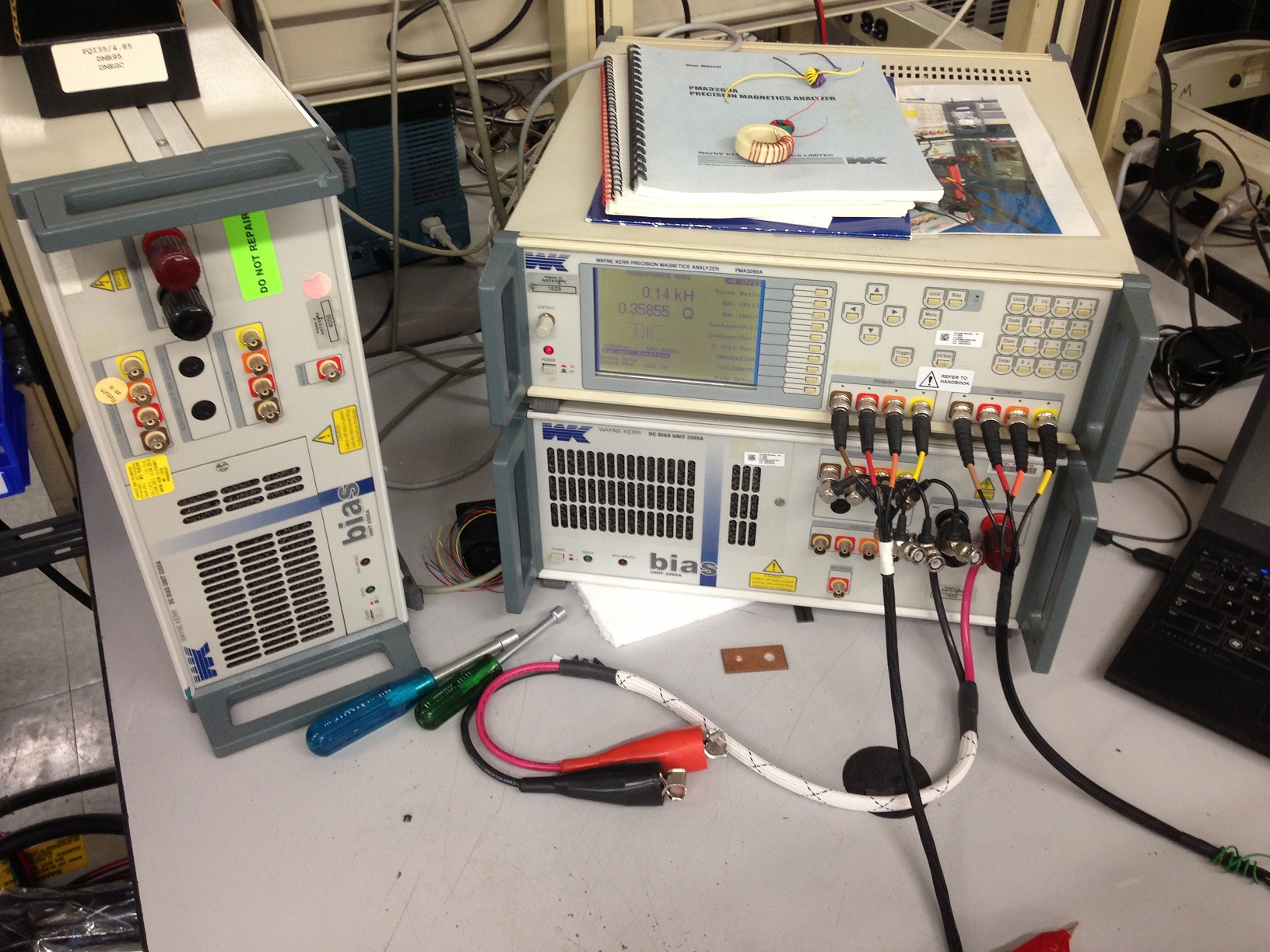 Wayner Kerr.JPG [ 661.33 KiB | Viewed 3783 times ]
tepples wrote:
Ben Boldt wrote:
Also, quick unrelated question -- I am looking at setting up a 240p Test Suite cartridge, which requires the unusual BNROM mapper.
240p Test Suite for NES comes in both UNROM and BNROM versions. UNROM can be built from incredibly common donors, but if you prefer the BNROM version, you can build BNROM out of an AN/AM/AOROM cartridge by cutting the 161's output corresponding to CPU D4 and running PA10 (vertical mirroring) in its place.
Oh, I didn't realize this, I will have to look into that. I have a damaged famicom "soccer" (NROM) that has been begging for something like this.
lidnariq wrote:
Ultron wrote:
but still, the crosstalk is lower than that.
I have to assume the ferrite there is to block a copy of the spurious emissions at some much higher frequency. Maybe at 3xcrystal = 64.4MHz ? It would be right in the middle of US NTSC channel 3.
Will do.
lidnariq wrote:
Ben Boldt wrote:
which requires the unusual BNROM mapper. I will need to make it out of an old NROM cart and 74HC161.
If you're starting with donors, any discrete logic mapper would be a suitable donor - UxROM, AxROM. Even MHROM/GNROM/CNROM if replacing CHR RAM is easier than adding a latch.
Quote:
Do you know how to hook up the '161? It must connect /ROMSEL and CPU R/W. I am thinking /ROMSEL goes to the clock input, and CPU R/W goes to /PE input?
Yes. /ROMSEL goes to ↑clock so that at the end of the cycle it'll latch the value on the data bus. R/W won't have changed yet by that time.
I will check around and see what carts I have, otherwise I will go ahead with the '161 in the soccer cart.
I will probably take apart my NES and dig out the ferrite bead, I do not want to touch my beloved AV famicom unless necessary... We have a big snowstorm here, it might be until this weekend or Monday to test the bead.
Ben Boldt wrote:
I actually did add an Amo-bead on the lead of the resistor connected to 5V. It had no visible effect when added in addition to the tantalum from 5V to GND. From what I understand, this is similar but different than a ferrite bead. They are definitely built different inside. We have these laying around everywhere, stuck in the cracks in the floor, etc, so I just grabbed one and threw it on to see what happened. Also, this is a very different location than you show in your circuit, Ultron.
I will try to locate the ferrite bead in my famicom, remove it, and measure it. We have a wonderful Wayne Kerr machine for measuring inductance and low resistance, perfect for this. At what frequency(s) would you guys be interested for me to measure this?
If you can, check 1MHz, 5MHz, 10MHz, 100MHz. If it goes down to 100kHz, check that too. We can get somewhat of a plot that way. That's some nice equipment!!
I have time to test some things this weekend in regards to the jailbars. I plan on removing the NESRGB from my top loader and adding AV again, so this would be a good time to test.
Do we expect the reactance to change as a function of frequency? I thought ferrites were comparatively ideal in that regard...?
lidnariq wrote:
Do we expect the reactance to change as a function of frequency? I thought ferrites were comparatively ideal in that regard...?
Yes, reactance changes with frequency in ferrite beads. I don't expect the bead to be the solution, but it would be nice to know its characteristics. If Ben Boldt has the time and access the equipment, it would be helpful.
Attachment:
 Ferrite Bead.png [ 72.31 KiB | Viewed 3757 times ]
X is the reactance in the plot.
Ultron wrote:
If Ben Boldt has the time and access the equipment, it would be helpful.
I can think of no better use of my time after work.

As I removed the ferrite bead from my USA NES, I noticed my big 2200uF cap was bulged! Glad we had a reason to go in there.
I took apart my AV famicom and verified that the ferrite bead looks exactly the same as the one I removed from the NES, and also that my AV famicom matches exactly your schematic Ultron.
I dug into both of my NES's and found that they are quite different than the AV famicom, and actually each of them even had different circuits than each other in the RF box... Both of them had an additional NPN transistor, and also a 3.3uH inductor involved. I am thinking that this extra stuff was due to tapping the video signal into the RF modulator. But since the AV famicom has the best video quality of them all (at least in my experience), I am not thinking that the NES's more complicated circuits are going to take us in a good direction.
I plan to do these things and see the difference at each step:
- change my resistor values to 300/110
- add the ferrite bead (after measuring it of course)
- add the 560pF cap
- Maybe try throwing in a 3.3uH and see what happens
Ben Boldt wrote:
I took apart my AV famicom and verified that the ferrite bead looks exactly the same as the one I removed from the NES, and also that my AV famicom matches exactly your schematic Ultron.
I dug into both of my NES's and found that they are quite different than the AV famicom, and actually each of them even had different circuits than each other in the RF box... Both of them had an additional NPN transistor, and also a 3.3uH inductor involved. I am thinking that this extra stuff was due to tapping the video signal into the RF modulator. But since the AV famicom has the best video quality of them all (at least in my experience), I am not thinking that the NES's more complicated circuits are going to take us in a good direction.
I plan to do these things and see the difference at each step:
- change my resistor values to 300/110
- add the ferrite bead (after measuring it of course)
- add the 560pF cap
- Maybe try throwing in a 3.3uH and see what happens
Yes, there were maybe 4 different RF boxes the NES used in its lifetime. Mitsumi made 2 of them I think (I have one with a Mitsumi). I did trace the circuit out for that one, just don't remember where I put it.
That's a good plan. I hope to do some testing this weekend too.
https://console5.com/wiki/Nintendo_NES-001 claims there were six different RF modulators used on the front-loader; three by Mitsumi and three by Alps.
I only know how to go up to 3 MHz with the Wayne Kerr. Here is the data:
Code:
Freq (kHz) | L (nH) | R (mOhm)
-----------+--------+-----------
3000 | 845 | 1200
2760 | 830 | 800
2500 | 815 | 600
2000 | 790 | 350
1500 | 778 | 250
1000 | 771 | 199
750 | 780 | 155
500 | 791.5 | 62.5
250 | 798 | 20
100 | 790 | -8
64.5 | 781 | -6
10 | 760 | 2.5
1 | 750 | 2.5
0 (DC) | n/a | 1.75
Attachment:
 inductance.png [ 10.05 KiB | Viewed 3666 times ]
Attachment:
 resistance.png [ 9.92 KiB | Viewed 3666 times ]
I played with this circuit some today, and I have some findings.
My circuit was actually pretty different than the AV famicom's circuit, it would not be apples-to-apples to change the resistor values. So I took everything apart and built the AV famicom circuit, skipping the ferrite bead and skipping the 560pF cap. I found that, without the tantalum from 5V to GND, this circuit starts out with much less jailbars, and the composite voltage is right bang on 1 Volt. Adding the tantalum still gives a big improvement though. (Scope shot shown with Tantalum)
Attachment:
 tek00008.png [ 94.05 KiB | Viewed 3659 times ]
I then added the 560pF cap, and I found that it squashed the signal a bit, making it less than 1V, and also the colors became less vibrant and just in general more muddy. I felt that it was in no way an improvement to add this cap, unless perhaps it is meant for ESD protection.
Attachment:
 tek00009.png [ 50.05 KiB | Viewed 3659 times ]
Next, I inserted the ferrite bead from my NES, the same one I tested above. I found absolutely no difference with or without this bead installed. Putting both the bead and the 560pF cap, was the same as just the 560pF cap and no bead. In no situation did I detect any difference from the bead. However, I am using good quality BNC cabling for all of this. Maybe crappier cables might benefit from the bead and 560pF cap, not sure.
I would say that the AV famicom, plus tantalum from 5V to GND, minus ferrite bead, minus 560pF cap is the simplest/best solution so far:
Code:
(GND)
PPU.20 ----------------+---------------------------------+
| | |
| | / (c) 2SA937 +----O } Composite
| PPU.21 --|< PNP } Video
| | ^ (e) 220uF +----O }
--- Magic | Electrolytic 110 |
--- Capacitor +----------|(---------/\/\/-------+
| |
| (+5V) 300 |
PPU.22 -------/\/\/----+
Ben Boldt wrote:
[tek00008.png]
That's zoomed out enough that I can't tell from that picture the extent to which that Vp-p is actually signal instead of noise on top of the signal.
Different TVs do different things on CVBS input. I was under the impression that they were only supposed to normalize to sync depth, but at least one other person here on the forum found that his TV also normalized chroma amplitude; in this latter case any attenuation by the extra capacitor that you're seeing on color would be normalized out.
Sorry, here is a better picture:
Attachment:
 tek00013.png [ 44.65 KiB | Viewed 11252 times ]
I am using a Kramer VP-413 connected to an LCD computer monitor. Looking more closely when adding and removing this cap, there is no loss in sharpness from it. There is a very fine, light checkerboard pattern on the whole display that goes away when adding this cap. The colors do get a little less saturated with the cap, but maybe that's a good thing, not sure.
Playing with my scope, I sure wish it could sync properly to this, but it's not looking like it can. The image just rolls. It seems to have some pretty awesome video features, I can zoom way in on the video (shown). Not useful without syncing. It doesn't let me control the syncing/trigger, it just lets me choose the options shown in this mode and none of them work right.
Attachment:
 tek00011.png [ 84.62 KiB | Viewed 11252 times ]
You've got a nice Tek scope there, I can't imagine they removed the "sync to NTSC scanline #X" feature that's in my crappy one (TDS1002)
Ben Boldt wrote:
There is a very fine, light checkerboard pattern on the whole display that goes away when adding this cap.
Does it look like that's the chroma carrier?
Oh it does have sync to line x in the trigger menu, but it can't trigger on anything with this signal. The best I can do is set the trigger to roll which allowed me to take that screenshot.
Here is without the 560pF:
Attachment:
 IMG_1680.JPG [ 239.06 KiB | Viewed 11245 times ]
Here is with the 560pF:
Attachment:
 IMG_1681.JPG [ 245.09 KiB | Viewed 11245 times ]
Ok, yeah, those artifacts look to me like chroma-into-luma bleed. I suppose the capacitor lowpass filters out some harmonic of the NES's square chroma signal.
Wow that's a nice o-scope. Thanks for taking the measurements, now at least we know that the bead is not a solution.
Are the last 2 shots you took with the top left corner with your tantalum bypass cap or without?
I do have to say, the composite out of the AV Famicom is WAY better than the NES or any console with the AV mod. It's like night and day.
Ultron wrote:
Wow that's a nice o-scope. Thanks for taking the measurements, now at least we know that the bead is not a solution.
Are the last 2 shots you took with the top left corner with your tantalum bypass cap or without?
I do have to say, the composite out of the AV Famicom is WAY better than the NES or any console with the AV mod. It's like night and day.
One of the advantages of my job is this great scope that I get to use, I love it. The last 2 shots were both with the tantalum bypass cap.
A basic question I have is that with the tantalum route, you do not need to lift the PPU Video Output pin to eliminate jailbars? That is a good thing if you do not have to do that.
So, if you want to improve the picture quality on an AV Famicom to make it sharper, you should remove the 560pF capacitor and the ferrite choke/bead and bridge the connection where the ferrite choke/bead was with a wire. Also, you should add a tantalum capacitor between +5v and GND, but is there any special place where you should put it? If I have read this thread correctly, then a 4.7uF 35V Tantalum
For the original Famicom, should we do something similar for simplicity's sake, build the AV Famicom's output circuit minus the 560pF capacitor and the ferrite choke/bead. The AV Famicom uses a 220uF 6.3V electrolytic capacitor and we can reuse the existing transistor. The 4.7uF 35V Tantalum should be added between +5v and GND as well with this older system.
Great Hierophant wrote:
and the ferrite choke/bead and bridge the connection where the ferrite choke/bead was with a wire.
No need. Ben Boldt didn't see any difference with the ferrite present/absent at all.
Okay, so you can keep the choke in place and limit the amount of work you have to do. Do you even need to add a tantalum to an AV Famicom? I can't see any jailbars in mine and I have looked hard for them. Do they become more noticeable once the 560pF is removed?
Great Hierophant wrote:
A basic question I have is that with the tantalum route, you do not need to lift the PPU Video Output pin to eliminate jailbars? That is a good thing if you do not have to do that.
I have not tried that yet. My pin is still connected in my test unit.
The 560pF seems to have no effect on the jailbars, but a finer grid pattern appears without it. lidnariq pointed out that this artifact is chroma-into-luma bleed. I would recommend using the 560pF. It dulls the colors slightly but does not make the image any more blurry. I also brought a typical cheap/thin yellow RCA cable with me today but I forgot to try it. I want to see if the ferrite bead makes a difference with that cable. I would not recommend making any change to a real AV famicom, Nintendo seems to have gotten it right with this model.
I have been having somewhat of a disaster of a night, not going too well. I finished wiring up the soccer cart into 240p Test Suite. It wasn't too bad, I had to use some copper foil to get at PPU /WR and CPU R/W but that went okay. I got home and went to program my W29EE512P-70 and found that my fresh Chinese PLCC-32 to DIP adapter had 2 (TWO) opens in it... Fixed that and programmed the chip. I put the cart in my Hi-Def NES and KABOOM, something blew up! No power with or without the cart in there now... Another project for another day. Hopefully fixable.
So I sat down with the cart, looked and probed for mistakes, shorts, etc, found
nothing. I bravely threw it into another NES, and it was okay, no explosions... Not sure what happened with the hi-def NES, no visible damage anywhere.
The 240p Test Suite PRG runs great. I did end up going with the BN-ROM approach, I used a 74LS163 that I had, which is compatible in this case. However, the CHR-RAM isn't working quite right.
Attachment:
 IMG_1682.JPG [ 185.94 KiB | Viewed 11051 times ]
The same tiles remain glitched when resetting, jiggling, etc. I used a UM6164AK-25 for the CHR-RAM. I tried swapping from the 'H' jumper to the 'V' jumper, that introduced additional problems, went back to H. I also tried swapping /OE and /CE on the RAM (PPU +A13 and PPU /RD), that made big problems, went back the way it was. I have a whole stack of these 6164s, I tried a different one and it didn't make a difference. Could -25 be too slow? Hmm... Anyway, it is good enough to use it for video testing purposes, just sort of a shame it is glitchy.
Attachment:
 IMG_1683.JPG [ 250.46 KiB | Viewed 11045 times ]
The NES PPU needs timing somewhere between 186ns (one pixel) and 372ns (two pixels), so I suppose the RAM speed might explain things?
In practice, the PPU timing has the address bus guaranteed stable after one half pixel (edit: 93ns) so as long as the RAM has a tCE-to-valid and tAddress-to-valid of not more than 280ns, and a tOE-to-valid of not more than 186, it really ought to work.
I have no idea what to make of that the bad picture is almost entirely made of sprites in the right place but with the wrong graphics.
These SRAMs came mysteriously in the bottom of a big bag of ISA and PCI cards, wrapped in aluminum foil. They appear to have been used before. It is possible that they are damaged.
Ben Boldt wrote:
The 240p Test Suite PRG runs great. I did end up going with the BN-ROM approach, I used a 74LS163 that I had, which is compatible in this case. However, the CHR-RAM isn't working quite right.
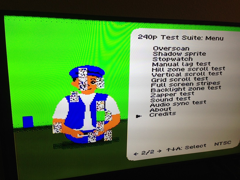
Based on that one blue sprite in Gus's vest that got displaced to the left side of the screen, I don't think that's a CHR RAM problem. It could be an OAM DMA problem. If it affected only tile number, a CHR RAM problem might be believable. But it affected one X coordinate, and that's copied straight from internal CPU RAM to the PPU's OAM data port.
tepples wrote:
Ben Boldt wrote:
The 240p Test Suite PRG runs great. I did end up going with the BN-ROM approach, I used a 74LS163 that I had, which is compatible in this case. However, the CHR-RAM isn't working quite right.
Based on that blue sprite in Gus's vest that got displaced to the left side of the screen, I don't think that's a CHR RAM problem. It could be an OAM DMA problem. If it affected only tile number, a CHR RAM problem might be believable. But it affected one X coordinate, and that's copied straight from internal CPU RAM to the PPU's OAM data port.
Very interesting, you have a great point. Did you notice the sprites that should be mirror images - in many cases one displays correctly, the other does not. This should be accessing the exact same CHR data. I just went and ran a few other games in this NES and verified that it is not broken.
Has anyone run the BN-ROM version on real hardware before? I am using 240pee-0.16.
Ben Boldt wrote:
Has anyone run the BN-ROM version on real hardware before? I am using 240pee-0.16.
I've run it on a PowerPak but not on a single-game cart. I've built a release candidate of 0.18, but that may not fix it.
I put it on there and it is slightly different. I uploaded a video so you can see how it flickers:
https://youtu.be/-aoXixJZXTY
It works great in the Famicom AV mod test unit...
Attachment:
 IMG_1685.JPG [ 182.07 KiB | Viewed 11034 times ]
- Hi-Def NES (USA Front Loader) -> Blows up, loud electrical snap noise right after I pressed the power button, then dead
- Unmodified USA Front Loader -> Sprite glitches
- Original Famicom -> Perfect
I did take apart the RF box on the Hi-Def NES just last week but also did power it on several times after reassembling. So I am not sure if it is related or not.
I also tried 2 different 72 <-> 60 pin cartridge adapters, both did the same thing in the unmodified front loader.
I find that the "color bars on gray" test makes the jailbars the most visible.
Here is a list of things I tried today, nothing of which made any observable difference:
- Cheezy video cable with and without ferrite bead (video quality was worse with the cable but unaffected by ferrite bead)
- Removed the 74LS373, installed socket, and changed to a 74HCT373
- Completely removed the RF box and powered the famicom directly with 5V bench supply
- Removed the PPU, installed socket, and did not connect video pin of socket to motherboard
- Inserted the ferrite bead first thing in the circuit, between PPU and base of transistor
- Shrunk the whole mod circuit -- used surface mount resistors and 560p very tightly on the bottom of the board
- Wrapping the PPU in copper foil, foil not connected to anything
- Connected the foil to all 5 GND pins (pin 20 and 14, 15, 16, 17)
- Added ceramic bypass caps directly from +5V pins (pin 40 and 22) directly to copper foil
- Sprinkled ceramic bypass caps all over the place on the bottom of the whole board
I also inserted a 3.3uH inductor at the very end of the circuit, i.e. pass the composite video through it. It made a slight difference but not an improvement.
At the end of all of that, I went back to Super Mario Bros. with all of these changes in place, I saw no difference from before. I am kind of out of things to try now, definitely open to trying any more ideas; I have only blown up 1 Nintendo this week.

So far, this is the best AV Mod circuit, and no crazy foil or cutting pins:
Code:
(GND)
PPU.20 ----------------+---------------------------------+--------+
| | | | Ring
| | / (c) 2SA937 560pF --- +----O } Composite
| PPU.21 --|< PNP Ceramic --- } Video
| | ^ (e) 220uF | +----O }
--- 4.7-47uF | Electrolytic 110 | | Pin
--- Tantalum +----------|(---------/\/\/-------+--------+
|+ | +
| (+5V) 300 |
PPU.22 -------/\/\/----+
One final copper foil test just to really put the nail in the coffin, since my PPU is in a socket and thus farther from the PCB, I put adhesive copper foil directly on the bottom of the PCB and under the whole mod circuit:
Attachment:
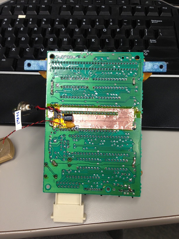 IMG_1689.JPG [ 204.39 KiB | Viewed 11004 times ]
No visible difference. We can call this myth busted.
I had some time today to do some testing.
I modded my top loader NES-101 to use the same circuit as the AV Famicom. Here is the stock video circuit for the NES-101:
Attachment:
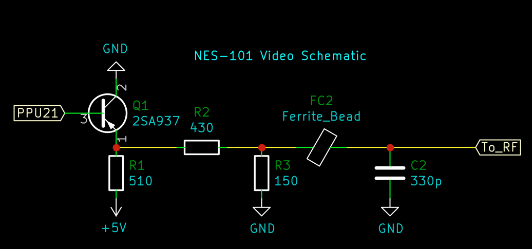 NES-101 Video.png [ 56.64 KiB | Viewed 10935 times ]
I replaced R1 with a 310 ohm resistor, and removed R2 and R3. In R2's spot, I connected a 220uF cap and FC2 in series.
Attachment:
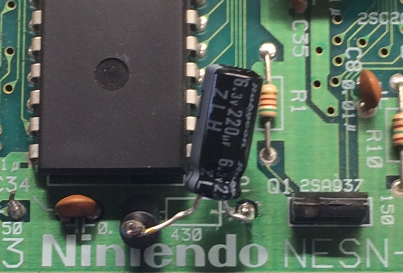 Cap and Bead.png [ 760.17 KiB | Viewed 10935 times ]
Then, I installed a 100 ohm resistor in FC2's spot.
Attachment:
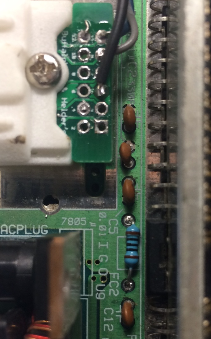 100 ohm.png [ 905.63 KiB | Viewed 10935 times ]
Then (with the RF unit removed), I connected the middle pin of the RF mod connection to Pin 9 on my multi-out. Connected multi-out GND (Pin 5) to a ground plane, wired up Audio to pin 11 and 12.
----------------------------------------------------------------------
For testing purposes, I used 240p suite on my Everdrive with a full screen color set to 00 (gray).
OK, so I took some o-scope and PVM screenshots of data. First, my unmodded AV Famicom:
Attachment:
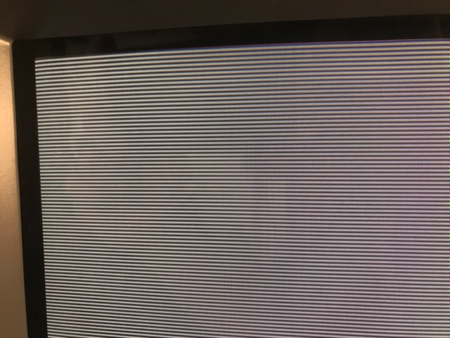 AV Fami Screen.png [ 492.3 KiB | Viewed 10934 times ]
And the active part of the video, zoomed in to look for noise:
Attachment:
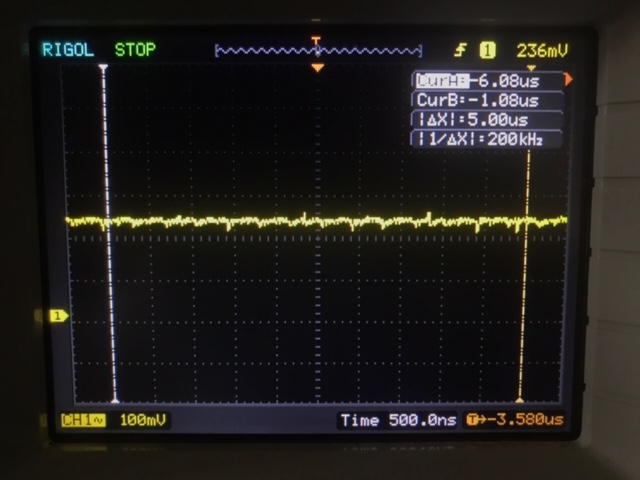 AV Fami Noise.png [ 370.28 KiB | Viewed 10934 times ]
As you can see, the image looks very clean, and there is no noise on the video signal.
Now, the NES-101, with the same setup as the AV Fami (First shot screen is blurry, but you can see the jailbars):
Attachment:
 NES-101 Screen.png [ 389.47 KiB | Viewed 10933 times ]
And the active video part:
Attachment:
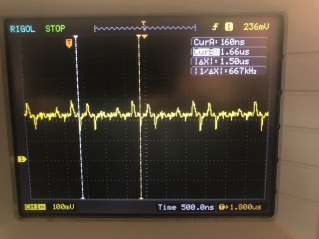 NES-101 Noise.png [ 396.96 KiB | Viewed 10933 times ]
Attachment:
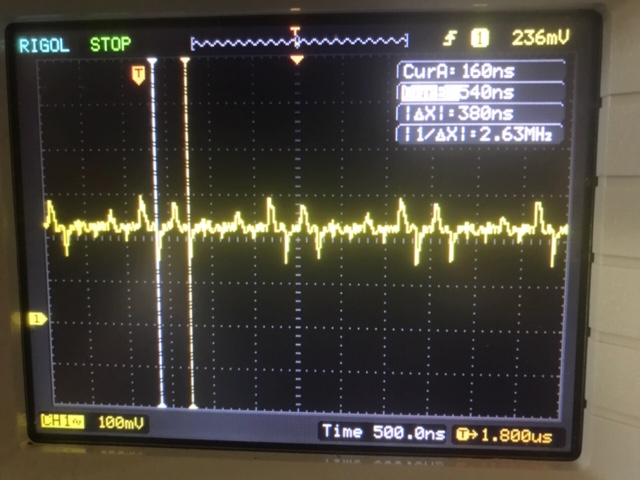 NES-101 Noise 2.png [ 464.91 KiB | Viewed 10933 times ]
So, you can see, the jailbars have an approx. 667kHz period, or approx. 8 pixels. The jailbar itself is approx. 2.63MHz period, or approx. 2 pixels in width.
EDIT: I should note, the measurements were taken on the left side of FC2 (negative side of the 220uF cap).
So why does modded NES-101 have jailbars and AV famicom perfect (as usual)? Does the AV famicom have a different PPU revision? I noticed when I had a wire attached to PPU pin 21, the other end not ever connected to anything, as I moved the wire around against the board, different jailbars would appear at different locations of this wire... But wrapping everything in foil proved not to keep the aliens out anyway. hmm Could this be a clock stability thing? Maybe each 8th clock pulse is a little wider or something? I never looked at that.
What part of the video signal are you looking at? Could you zoom out to a whole scanline or frame and circle the area you were looking at? I am a little confused and not very familiar with composite video. It looks like you have a great way to measure the jailbars, I would like to repeat that with my setup. Everything I did was qualitative by eye looking at an LCD monitor -- I would love to have a reliable way to actually measure it.
Ben Boldt wrote:
So why does modded NES-101 have jailbars and AV famicom perfect (as usual)? Does the AV famicom have a different PPU revision?
No, the 2C02 G-to-H transition happened in both markets about the same time, and IIRC happened before the NES-101.
Quote:
I noticed when I had a wire attached to PPU pin 21, the other end not ever connected to anything, as I moved the wire around against the board, different jailbars would appear at different locations of this wire... But wrapping everything in foil proved not to keep the aliens out anyway.
I think PCB layout is the biggest factor here... which may be why there's so much superstition. You're using basically the same amplifier as the original, but it's in a different place.
Quote:
Could this be a clock stability thing? Maybe each 8th clock pulse is a little wider or something?
That wouldn't cause this particular kind of artifact...
Quote:
I would love to have a reliable way to actually measure it.
Use something with white or grey instead of color - the color carrier will make it hard to see the comparatively smaller magnitude jailbars.
(this was my 8255th post, a GPIO expander used as the keyboard interface in the original IBM PC)
lidnariq wrote:
I think PCB layout is the biggest factor here... which may be why there's so much superstition. You're using basically the same amplifier as the original, but it's in a different place.
I guess I am surprised that bad layout isn't made better with these copper foil attempts. I have grounded copper foil completely between my amplifier and the PCB. Interesting to think where this could be getting in and where from.
lidnariq wrote:
That wouldn't cause this particular kind of artifact...
Okay
lidnariq wrote:
Use something with white or grey instead of color - the color carrier will make it hard to see the comparatively smaller magnitude jailbars.
That was my plan all along, I had lost track of that! I have the 240p Test Suite cart, I just never ran a white screen and looked at it with the scope. I will do that next chance I get.
Ben Boldt wrote:
So why does modded NES-101 have jailbars and AV famicom perfect (as usual)? Does the AV famicom have a different PPU revision?
Because the NES-101 has the worst PCB layout known to man. A first grader could have done a better job of laying out the traces. My NES-101 has a -G, the AV Fami is -H. Though I don't think that matters (I can swap the PPUs and I'm sure it won't make a difference).
The decoupling scheme is horrible. There is no decoupling cap anywhere near the power pin of the PPU. I added a 0.1uF ceramic, but this did not make a difference. It may need some more decoupling.
Quote:
hmm Could this be a clock stability thing? Maybe each 8th clock pulse is a little wider or something? I never looked at that.
A lot happens on the 8th pixel of every line. Tiles are 8x8 pixels, so the PPU is doing a lot of work every 8 pixels. Because of this, I believe the noise is coming from a current surge, not necessarily from a noisy pin or trace. I also need to check other pins nearby. I can see some noise on the PPU power pin (Pin 40) of this frequency. Though not as large as on the video signal, the noise does pop up on the 5V line; the noise is MUCH less in amplitude on the AV Fami.
Quote:
What part of the video signal are you looking at? Could you zoom out to a whole scanline or frame and circle the area you were looking at? I am a little confused and not very familiar with composite video. It looks like you have a great way to measure the jailbars, I would like to repeat that with my setup.
I am looking at the active video part. Like lindariq said, use a white or gray screen in 240p suite. The active video part is located after the color burst.
Attachment:
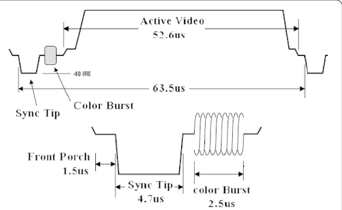 Composite Video.png [ 56.53 KiB | Viewed 10831 times ]
Even with the crap layout of the video path on the PCB, I don't think it's picking up interference from it. When the Everdrive starts up, it flashes a blue and green screen, before showing the menu. The blue and green screens DO NOT have jailbars on them. The menu does, though.
I have a very good view of the jailbars now with white screen. I believe that the jailbars are apparent each time there
isn't a ripple with my setup.
Attachment:
 tek00014.png [ 46.69 KiB | Viewed 10581 times ]
Quite fascinating, when I apply a 1k pull-down on the ALE signal, the ripple reduces:
Attachment:
 tek00015.png [ 44.62 KiB | Viewed 10581 times ]
I can't visually tell a difference on the white screen though. If I apply a 1k pull-up, it has no effect. If I put a 0.1uF ceramic cap in series with the pull-down, it creates the same reduction in ripple. Comparing 74LS373 to 74HCT373 with this setup, I see no measurable difference. While running, if I completely yank out the 74x373, it also has no effect on the ripple. (Amazing to me that it keeps running that way...) Since ALE is only connected to the '373, these clues seem to point to noise entering through the ALE pin, or being generated by the ALE pin. I tried the 1k and cap, pull-up and -down on all other pins and found no similar effect elsewhere.
Notice the correlation between the PPU AD pins and the ripple. The ripple does not occur at the points where the PPU AD pins don't change. Since the only other thing these are connected to is the PPU's SRAM, it might be interesting to swap SRAM chips and see what happens.
Ben Boldt wrote:
Since the only other thing these are connected to is the PPU's SRAM, it might be interesting to swap SRAM chips and see what happens.
May as well just try pulling it altogether. Won't be any more wrong than removing the '373.
lidnariq wrote:
Ben Boldt wrote:
Since the only other thing these are connected to is the PPU's SRAM, it might be interesting to swap SRAM chips and see what happens.
May as well just try pulling it altogether. Won't be any more wrong than removing the '373.
Ooo neat idea, I like it. I will dig around for a narrow DIP-24 socket, I am sure I have one somewhere.
Edit:
I must have used my last damn dip-24 socket for the RAM in that 240p test suite cart... There aren't any left where I usually store them. I will order some and keep looking. 50% chance I will find 100 of them right after ordering more.
Edit 2:
I ordered various sizes last night, and sure enough, I found tons of some of the ones I ordered. But no narrow dip-24s... I have plenty of wide dip-24s and narrow DIP-28s, but not too excited to go that route. I will keep looking.
Edit 3:
Turns out that RAM chip I put into the 240p cart is actually a dip-28, so it looks like I never had any narrow dip24s to begin with.
I put this off for so long that I actually got the correct sockets in the mail. I pulled the RAM chip with it running, and while it does glitch everything up, it seems to still have the jailbars amidst the garbage on the screen. I also ordered a CY7C128A-25PC SRAM chip (25 nsec). I will be able to take measurements comparing the original RAM to this new one. And as a matter of fact, both this famicom and my broken Hi-Def NES have socketed PPUs, so I can swap the PPUs too and see if anything measures differently.
Edit:
I just threw the other PPU in there for the heck of it and interestingly, it has the sprite glitch now with this PPU. So both of my front loader PPUs have this glitch.
On the top loader NES-101, I was able to clean up the +5V signal by replacing almost all electrolytic caps with polymer electrolytic capacitors (I replaced the ones that mattered in this situation - Power). I replaced the main filter cap and the cap near the cartridge slot. I also added a 47uF in place of C35 (which was just a decoupling capacitor located way too far away from the PPU Pin 40 to do anything). This reduced the noise on Pin 40 of the PPU, but DID NOT change the noise on the video output. The noise on the Pin 40 was reduced from ~60mV pk-pk to ~20mV pk-pk. I picked the 47uF cap due to its impedance curve. Pin 40 now looks much like the measurement I took on the AV Famicom.
Before (same pic as in one of my posts above):
Attachment:
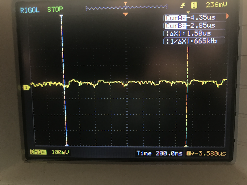 5V-Before.png [ 755.14 KiB | Viewed 12173 times ]
After:
Attachment:
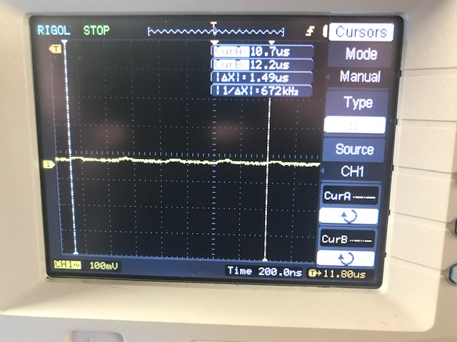 5V-Clean.png [ 472.11 KiB | Viewed 12173 times ]
Board:
Attachment:
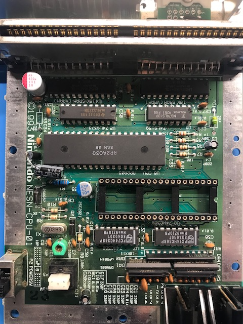 Poly Caps.png [ 631.37 KiB | Viewed 12173 times ]
I also tested PPU revisions by swapping in my -H from the AV Famicom into the NES-101. Noise was still there. In fact, the -G from the NES-101 I installed in the AV Famicom produced clean video output. Which concludes that the PCB layout is the issue, not the PPU revision.
I agree that it sounds like a layout thing. What could it be about the layout that causes the problem? From my experience in noisy environments, I have found that there is always a possible kludge once the problem is understood. Sometimes the kludge comes first before we understand it! That's kind of what I have been looking for as I poke around. Sticking resistors and caps at different places, adding sockets, yanking/swapping chips, etc. Something is bound to have an interesting effect.
We know that the jailbars are stationary and synchronized to when the PPU accesses memory. That is a really big important fact. What path does it take to make its way out to the video signal? In terms of EMI, is it conducted (through wires) or radiated (through the air)?
You and I have both shown that better decoupling caps greatly improves the situation. Is there still something on the power rails somehow? Ground loops? Inductance of the PPUAD traces? I am at a loss.
Ultron wrote:
This reduced the noise on Pin 40 of the PPU, but DID NOT change the noise on the video output.
This is a very interesting observation. It points to the jailbars being picked up IN or AFTER the video amp, which could include the television set itself. Does the NES-101 have a metal shield like the AV famicom?
Ben Boldt wrote:
I agree that it sounds like a layout thing. What could it be about the layout that causes the problem? From my experience in noisy environments, I have found that there is always a possible kludge once the problem is understood. Sometimes the kludge comes first before we understand it! That's kind of what I have been looking for as I poke around. Sticking resistors and caps at different places, adding sockets, yanking/swapping chips, etc. Something is bound to have an interesting effect.
We know that the jailbars are stationary and synchronized to when the PPU accesses memory. That is a really big important fact. What path does it take to make its way out to the video signal? In terms of EMI, is it conducted (through wires) or radiated (through the air)?
You and I have both shown that better decoupling caps greatly improves the situation. Is there still something on the power rails somehow? Ground loops? Inductance of the PPUAD traces? I am at a loss.
I believe it's the way the ground plane is laid out. The PPU does heavy switching on it's output pins. The large changes in current due to the switching need a large ground plane to help dissipate these spikes. I don't think the ground plane in the area of the PPU is large enough. I believe this to be the problem in both the Famicom and NES-101.
Another thing is, in circuit design, you learn to keep analog and digital ground paths separate from each other, and only tie them together at the power source (or power connection). Since the PPU is doing double duty by reading in pixel data and producing a video signal, and only has one GND pin, you would point to this. But, the "jailbar" noise is much less on a toaster NES (it is there, I have measured the video signal), and non existent on the AV Famicom, which both use the same PPU. So, it's safe to say the PPU itself isn't the source of the problem. What would happen if you removed the PNP transistor for buffering and tied it's collector (which should be tied to "analog" ground) to the regulator ground pin, or a different section of the ground plane? I wonder if this would help.
I think the real fix would be an adapter board, with the PPU mounted on it, some decoupling MLCC caps, and a nice large ground plane. The board could be mounted where the PPU normally sits, with the EXT and GND pins on the main PCB tied to the ground plane on the adapter board. The question would be how to fit it into the Famicom case.
Quote:
This is a very interesting observation. It points to the jailbars being picked up IN or AFTER the video amp, which could include the television set itself. Does the NES-101 have a metal shield like the AV famicom?
Yes it does, but those metal shields wouldn't help in this case. All my tests were with them removed, and the AV Famicom still comes clean.
Just to show you the noise on the GND pin of the PPU on the NES-101 (using the heat sink as a reference):
Attachment:
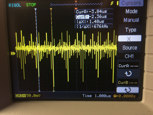 PPU GND Noise.png [ 474.63 KiB | Viewed 12140 times ]
Meanwhile, the CPU GND pin is clean as a whistle:
Attachment:
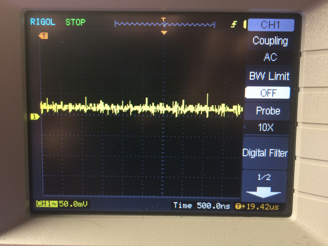 CPU GND Noise.png [ 448.08 KiB | Viewed 12140 times ]
You can see the ~676 kHz noise on the GND pin, which is every 8th pixel, the same noise seen on the video.
Wow, I think you are really onto something with that. This high frequency stuff can be sneaky though, depending how you were probing it, you may have formed a loop large enough to pick up radiated stuff. But it really does prove a point.
When I wrapped one of my PPUs in copper foil, I soldered all GND pins directly to the foil and put ceramic bypass caps directly from the 5V pins to the copper foil as well. This forms a very low impedance local ground plane. I did all of the soldering on the top of the chip, so it does not interfere with any of the pins going into the socket. None of that seemed to have any visual effect but I did not measure the composite signal at the time that I did that. When I swapped the shiny copper PPU to the bare one from my front loader, again it is visually the same on the screen. Sorry for not taking measurements lately.
To your point, I didn't connect my copper foil to any sturdier ground anywhere. I wonder if something good might happen if we connected some thick wire between various GNDs and 5Vs. Some SNES video improvement guides suggest adding some wire like this.
Ben Boldt wrote:
Wow, I think you are really onto something with that. This high frequency stuff can be sneaky though, depending how you were probing it, you may have formed a loop large enough to pick up radiated stuff. But it really does prove a point.
When I wrapped one of my PPUs in copper foil, I soldered all GND pins directly to the foil and put ceramic bypass caps directly from the 5V pins to the copper foil as well. This forms a very low impedance local ground plane. I did all of the soldering on the top of the chip, so it does not interfere with any of the pins going into the socket. None of that seemed to have any visual effect but I did not measure the composite signal at the time that I did that. When I swapped the shiny copper PPU to the bare one from my front loader, again it is visually the same on the screen. Sorry for not taking measurements lately.
To your point, I didn't connect my copper foil to any sturdier ground anywhere. I wonder if something good might happen if we connected some thick wire between various GNDs and 5Vs. Some SNES video improvement guides suggest adding some wire like this.
Yes, I agree with picking up noise with "how you probe it". Most of my measurements were done with a ground spring on the o-scope probe, which is the best way to do it. The GND measurements obviously were not done that way, but you would figure that the noise would show up on both grounds if the probe was picking up interference.
I'm not sure if the copper foil would do the trick. Maybe it is too thin?
I did try adding a ~22 gauge wire between pin 20 and a different spot on the ground plane. This seemed to make a little difference, but not as much as I would have hoped.
I think I'm giving up on the NES-101 for now, and will move on to the Famicom to see what I can do.
Ultron wrote:
The GND measurements obviously were not done that way, but you would figure that the noise would show up on both grounds if the probe was picking up interference.
You can test that if you connect the probe tip directly to probe GND and nothing else, and hold it approximately where you were probing before. Whatever
doesn't show up this way was your true difference in GNDs.
Ultron wrote:
I'm not sure if the copper foil would do the trick. Maybe it is too thin?
Good point. This is some pretty thin stuff I used. I cut it easily with a scissors and X-acto knife.
Ultron wrote:
I did try adding a ~22 gauge wire between pin 20 and a different spot on the ground plane. This seemed to make a little difference, but not as much as I would have hoped.
Was this a visible difference on the screen, or was it a difference on your scope?
Ugh, I don't know how I did this but I got my CY7C128A chip last night to find that it is not even the right number of pins! Here I was thinking I could just plug the thing in and it would work. Silly me. We kind of disproved the RAM chip anyway but just thought I would post an update on that...
Edit:
Heyyyyyy! The datasheet shows a 24-pin chip and this is 28-pin! LOL I wonder what the heck is going on here.
Edit 2: The picture of the item is 24-pin. Hmm...
Conrad7K wrote:
I think tantalum might not be the best choice here, they work their magic best on voltage rails and things that always stay positive.
For the bypass cap (i.e, the one directly from 5V to GND), I found that using a tantalum produces the best results, and there is nothing that should ever make that cap go negative, so I really do recommend tantalum for that cap.
With the large series cap, I found that using a tantalum isn't really any better than using an electrolytic. From what I understand, this cap never goes backwards either though. Think about it like this: the signal before this cap ranges from 0V to +1V. After the cap, the signal ranges from -0.5V to +0.5V. So, at all times, the cap basically has a constant DC -0.5V across it, then the whole cap floats along with the signal, not really seeing the signal internally. Since it is holding a flat -0.5V, you put it in backwards and it should always be happy. To your point, I would recommend electrolytic for this one, especially for unknowns like when you plug and unplug the video jack, etc, but I think in general a tantalum would actually still be OK.
Hello, I want to attempt the AV mod on my Famicom as described in this latest method that you guys have figured out. Just some questions about the tantalum capacitor part:
1. Where did you solder it, the top or the bottom of the motherboard? I didn't see it in the picture that was in this post, so just wondering where I'm supposed to add the capacitor (I have barely worked with soldering anything and I didn't learn any more electrical stuff outside of high school physics, so I'm pretty new to some of this)
2. Does the uF number of that capacitor matter (between 4.7 and 47 as previously experimented with)? Like, is it better to have it higher?
Otherwise, this looks like a really good mod, I really appreciate that it is non-destructive and pretty easily reversible (other than needing to remove and re-purpose the transistor)

progress in 2019 is awesome
Anomunus wrote:
Hello, I want to attempt the AV mod on my Famicom as described in this latest method that you guys have figured out. Just some questions about the tantalum capacitor part:
1. Where did you solder it, the top or the bottom of the motherboard? I didn't see it in the picture that was in this post, so just wondering where I'm supposed to add the capacitor (I have barely worked with soldering anything and I didn't learn any more electrical stuff outside of high school physics, so I'm pretty new to some of this)
In this photo (
download/file.php?id=15358&mode=view), it is the yellow Tic Tac-shaped component.
Anomunus wrote:
2. Does the uF number of that capacitor matter (between 4.7 and 47 as previously experimented with)? Like, is it better to have it higher?
I found that higher is
not better. I noticed the quality got slightly worse with less than 4.7uF and also slightly worse with greater than 47uF. In general, larger capacitors are better at lower frequencies, and smaller capacitors are better at higher frequencies. I wouldn't say that we proved it, I certainly didn't get a PHD in that stuff but it seems reasonable that the range 4.7-47uF is tuned for whatever frequency(ies) are involved here. You would want to use any one of these common values:
4.7uF (475)
6.8uF (685)
10uF (106)
15uf (156)
22uF (226)
33uF (336)
47uF (476)
If you want me to tell you a specific value, go for 22uF 16V. But really I could tell no difference between any of those I listed above, so if you can find one from the list on an old motherboard or hard drive or LCD or something, it will be just as good. Special note: unlike electrolytics, the stripe means (+) on tantalums. It is very important not to get it backwards.
Do these rules also apply to clones or they're completelly different beasts?
PPU clones probably have the same reason for the problems Ben Boldt and Ultron outlined here. The decapped UA6538 is very similar layout-wise to the real 2C02.
Famiclone PCBs will probably have different layout than the top-loader, so might need additional fortification of the power supply to the PPU beyond just a capacitor.
Good to know.
I have a clone wich have a "stereo headphone" output.
It's nice and had a bunch of problems that I could fix, but now it has 2 horizontal lines that passes on screen.
Looks like it's a power supply problem, because they vanish if I remove the audio module.
It uses an LM317 instead of a 7805.
I'll open a new thread to discuss this as soon as I can get some more information in digital form about it's circuit.
Two
horizontal lines? That's almost certainly a power supply filter issue, and you probably just need to replace the capacitors in there.
What Ben Boldt and Ultron were investigating was a pattern of vertical lines, like what Ben Boldt showed
here.
Thanks for the tip.
Changing the capacitors made it way better, but still not perfect.
Interestingly the NROM and UNROM games I tested show no lines, while most games that use more complex mappers like MMC3 and VRC4 still show them after a while.
I made small resistor changes on the video and audio output to get a brighter image and louder sound, not sure if this can be causing the issues.
I must take a look at the schematics I found and write wich resistors I changed and post here to give an better idea of what was made.
I'll do that as soon as I can.
Could you share a photo of the horizontal lines? Do you hear a humming in the audio? Maybe it could be a ground loop also.
Yes, it has a hmmm on it.
It got a little better after the recap, but it's still there.
Here's a screenshot:
Attachment:
File comment: I think this shows the bar pretty well.
 tvtime-output-184334.png [ 1014.69 KiB | Viewed 1023 times ]
And here is the console:
Attachment:
File comment: Dynavision 3
 20190928_173741.jpg [ 494.82 KiB | Viewed 1023 times ]
His guts:
Attachment:
File comment: Guts 1
 20190928_173848.jpg [ 610.68 KiB | Viewed 1023 times ]
From another angle:
Attachment:
File comment: Guts 2
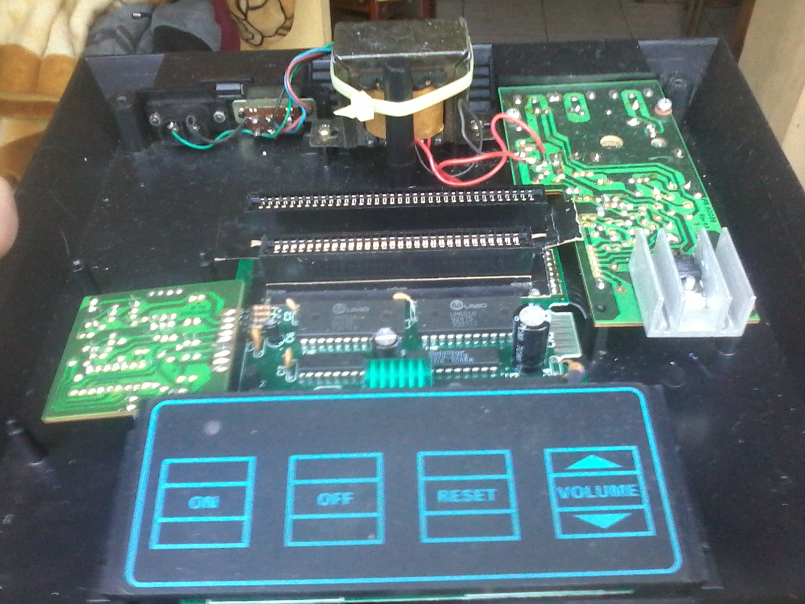 20190928_173859.jpg [ 701.91 KiB | Viewed 1023 times ]
The problems disappear if I remove the board on the left, wich is comprised of a volume controller IC (Toshiba TC9153AP) and some transistors for audio amplification:
Attachment:
File comment: Audio comp.
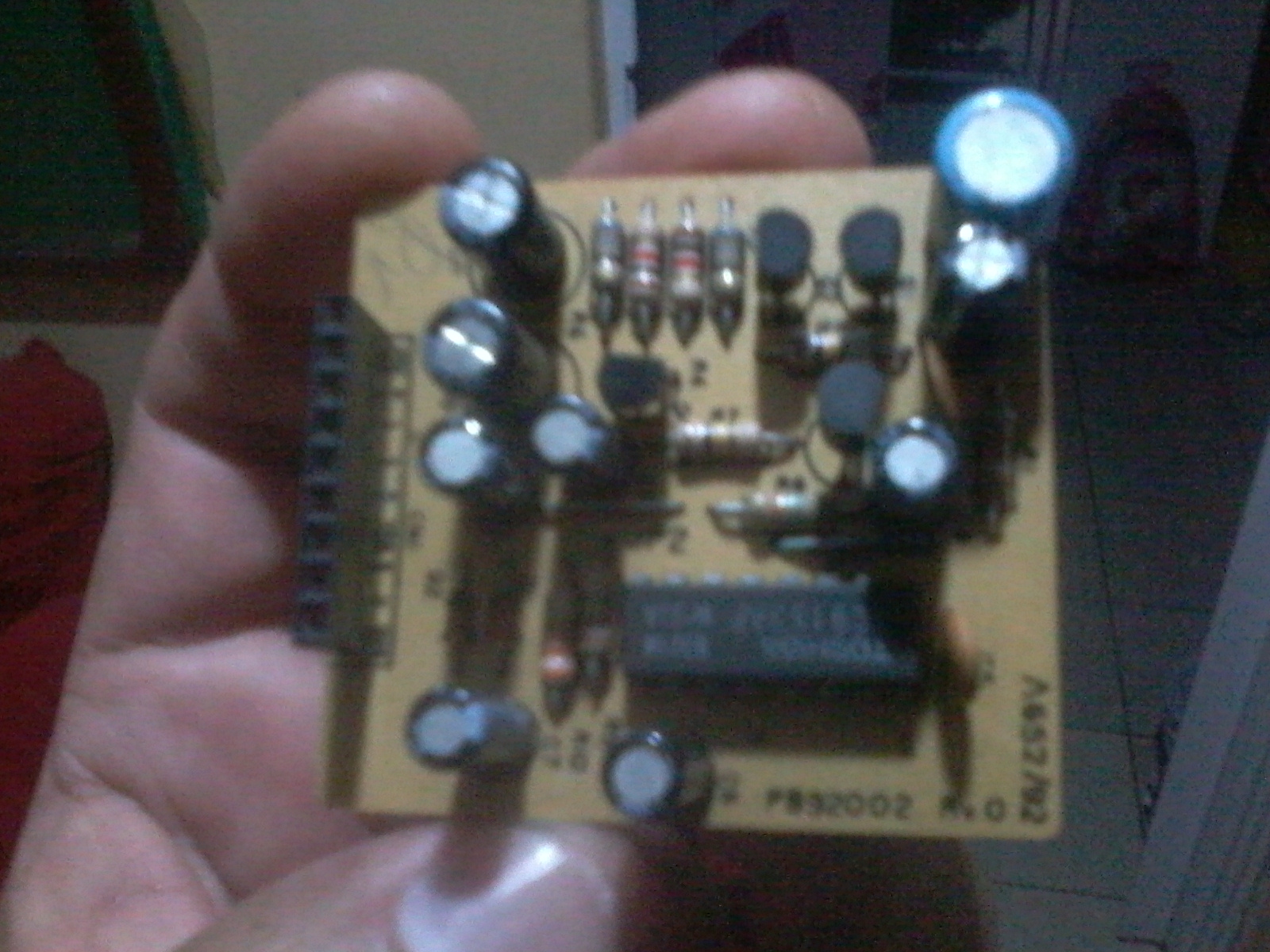 20190928_190056.jpg [ 591.45 KiB | Viewed 1023 times ]
I couldn't add the other side of the PCB, sice 5 images is the limit.
Let me know if it's necessary.
I think I drawed this PCB's schematics some time ago, but I can't find it right now.
Probably it's a ground loop, wich I have no idea on how to solve.
Any help will be welcome.
Thanks in advance.
That sure looks like a ground loop to me. Does the horizontal bar scroll or is it always at the same spot? (Not sure what that would exactly tell us but the console's video generation should not be perfectly synchronized to the AC line voltage.) You could try different/shorter A/V cables or cleaning the connectors. Maybe try a different power adapter.
Frame rate on Brazilian Famiclones (ones that emit PAL-M natively) should be 60.03Hz, so should have a 31 second beat pattern (compared to the 17-second beat pattern that "real" NTSC has, the 10 second beat pattern than the 2C02 has, or the 143-second beat pattern that the 2C07 has)
Yes, it scrolls down, when it reaches the botton it appears again at the top.
I've already tried a few cables and even other outlet.
The power supply is internal.
Maybe if I try to substitute the transformer with a switching power supply?
The interesting thing is that all this vanishes if I remove that small daughterboard.
I've found some schematics.
Here's the mainboard:
Attachment:
Here's the power supply and the audio board:
Attachment:
AFAIK, these schematics are from different PCB revisions from mine, I noticed:
- The motherboard is exactly the same on these schematics.
- The power supply board has some components numbered slightly different, probably due to the RF generator being changed to a RF module.
- The audio board is totally different than mine, not sure wich would be better.
I did some small changes to get better image and sound on my TV:
- I changed R12, that's on the base of the video out transistor, from 15K to 10K, with this the image that was too dark became "normal".
- I changed R28, that sits just before the audio output, from 5,5K to 1K, with this the audio became louder.
Could these changes be causing this trouble?
Looking at connector CN2, presumably this comes off of a transformer, with the center tap connected to GND. It then rectifies the AC from the transformer using D1 and D2, and peak charges C6, which is the large 2200uF capacitor. With this type of power supply, there is always a 120Hz ripple which increases with more load. If C6 is going bad, the ripple will get worse, and will improve by removing load, i.e. removing the audio board. Based on your description of 2 large horizontal bars that scroll slowly, it makes sense.
The NES and Famicom have a similar large 2200uF 25V capacitor. With all of these old systems, I highly recommend replacing this capacitor even if it isn't bad yet or doesn't solve a problem anyway. I think there is a chance that this is what is wrong with yours. I could only see 1 horizontal bar in your photo, and I would expect 2 if C6 is bad but it is just going to be a good idea to replace that old capacitor anyway, worth a shot.
Well, when I recapped it I already changed this capacitor.
Should I put a bigger one?
Strangelly I remember the 2 bars, but also only saw only 1 this time.
Maybe it was before the recap.
It was a while ago, I was with very little free time to get info and look for help.
I've found the draw I did from the audio board:
Attachment:
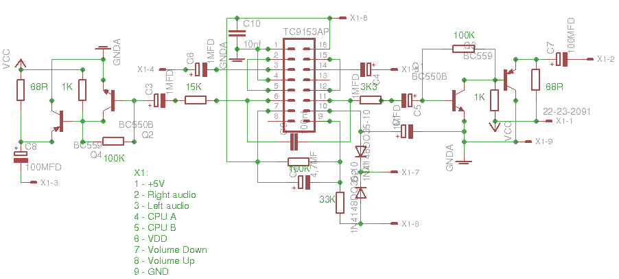 Audio board.png [ 14.87 KiB | Viewed 977 times ]
Not the best draw and probably has some mistakes, but it's what I have for now...
I'll try to get some "naked" scans for that board.
Maybe it's not needed since it's a single face PCB, 2 good pictures probably will do the same job.
Interestingly there's a V- signal that powers a flipflop.
There's also a smaller rectifier circuit with a BC549 and a zener wich gives the VDD.
AFAIK the VDD is there to make the volume IC "remember" the last volume level.
I tought this could be the cause and tried to unplug this pin on the audio PCB with no change.
Fisher wrote:
Well, when I recapped it I already changed this capacitor.
Should I put a bigger one?
Strangelly I remember the 2 bars, but also only saw only 1 this time.
Maybe it was before the recap.
Bummer. You could experiment by taking an additional cap and attaching it temporarily. You could also try that across the negative voltage rail (i.e. C20, 100uF). But I am thinking that now it pretty much points back to some sort of a ground loop.
I am not sure if I have understood something quite right. I know when you remove the audio board the problem goes away. Did I hear you say that also if you disconnect the external audio cables (with the board still installed), it also makes the problem go away? If so, maybe that is a clue.
I tried to unplug one or other of the AV cables without success.
Them I tried to add a 1000mfd x 16v together with C6 and the bar got softer.
Since the next bigger one I had around was a 4700 x 25v I added it and the bar vanished.
I think it's a bit overkill, but seems to have solved it.
Still needs more extensive testing but looks OK.
Another doubt I have is how can I add the extra Famicom audio to the headphones.
I tried to use some resistors, but they either muted the extra audio or made the whole audio distorted.
maybe I should use a transistor?
lidnariq wrote:
Two
horizontal lines? That's almost certainly a power supply filter issue, and you probably just need to replace the capacitors in there.
What Ben Boldt and Ultron were investigating was a pattern of vertical lines, like what Ben Boldt showed
here.
I totally missed that post, sorry
I'm aware that I'm going pretty much off topic here, and even intended to open a new thread. But since we're already discussing it here, I let it go.
Your idea about the capacitor was correct. Not sure why the full recap didn't solve everything at the beginning.
Not very good capacitors maybe?
The voltage at C6 might be more than 16V. You can't get away with a 16V cap in a real NES, I tried that once and it did vent after a while. Not sure about this console though. Increasing this cap in uF and voltage sounds like a good upgrade to me.
Indeed a great upgrade!
Even the jailbars are very soft now!
Attachment:
File comment: Fester's jailbars
 0fcc8dcc-601f-4c8d-8b2b-3ad22be0d5ce.jpeg [ 130.04 KiB | Viewed 879 times ]
It was great to finally finish the fixing of this console.
I bought it as non-working at the beginig of the year.
It had many problems: burnt CPU, bad VRAM and a couple bad transistors.
The knowledge I used to fix it was almost all here at the forums.
In fact, I asked only about that last one because I was afraid it was a ground loop, wich I had no idea on how to start looking.
It still has some noise at the audio, but I think it's due to the design.
Unfortunatelly I have not much time to search for a "cure", so let it stay this way.
So thanks to you guys it now works perfectly.
Ben Boldt wrote:
If you want me to tell you a specific value, go for 22uF 16V. But really I could tell no difference between any of those I listed above, so if you can find one from the list on an old motherboard or hard drive or LCD or something, it will be just as good. Special note: unlike electrolytics, the stripe means (+) on tantalums. It is very important not to get it backwards.
Hey just returning to share my results of building your circuit (as you previously showed
here) with the tantalum you specified. My original intention of doing the AV mod was to see if I could fix my Famicom's being unable to show a colour image when I was using its RF output. Unfortunately it's still black and white (which means something else is wrong with it, and I don't know what), but the resulting image from this design is definitely sharper than the RF output. Also, can't tell if there's any jailbars honestly.
My implementation allows the board to fit back into the case perfectly; combined with my unacceptably poor soldering skill this meant having to lengthen the circuit a bit in order to make the components fit into place, as well as changing one key component.
I used the same resistors and 560pF ceramic specified. For the 2SA937 transistor that is supposed to be re-used, I failed to get it off the board properly (ended up accidentally tearing it off at all the legs). I replaced it with a NTE290A (equivalent to 2SA1015 which is apparently used in the Twin Famicom and has been used in this mod found
here). The electrolytic capacitor is 220uF 35V. The tantalum is 22uF 25V.
Attachment:
File comment: The Hong Kong Famicom lacks a channel switch, so I am able to wire the RCA plugs through that hole without cutting the case in any way!
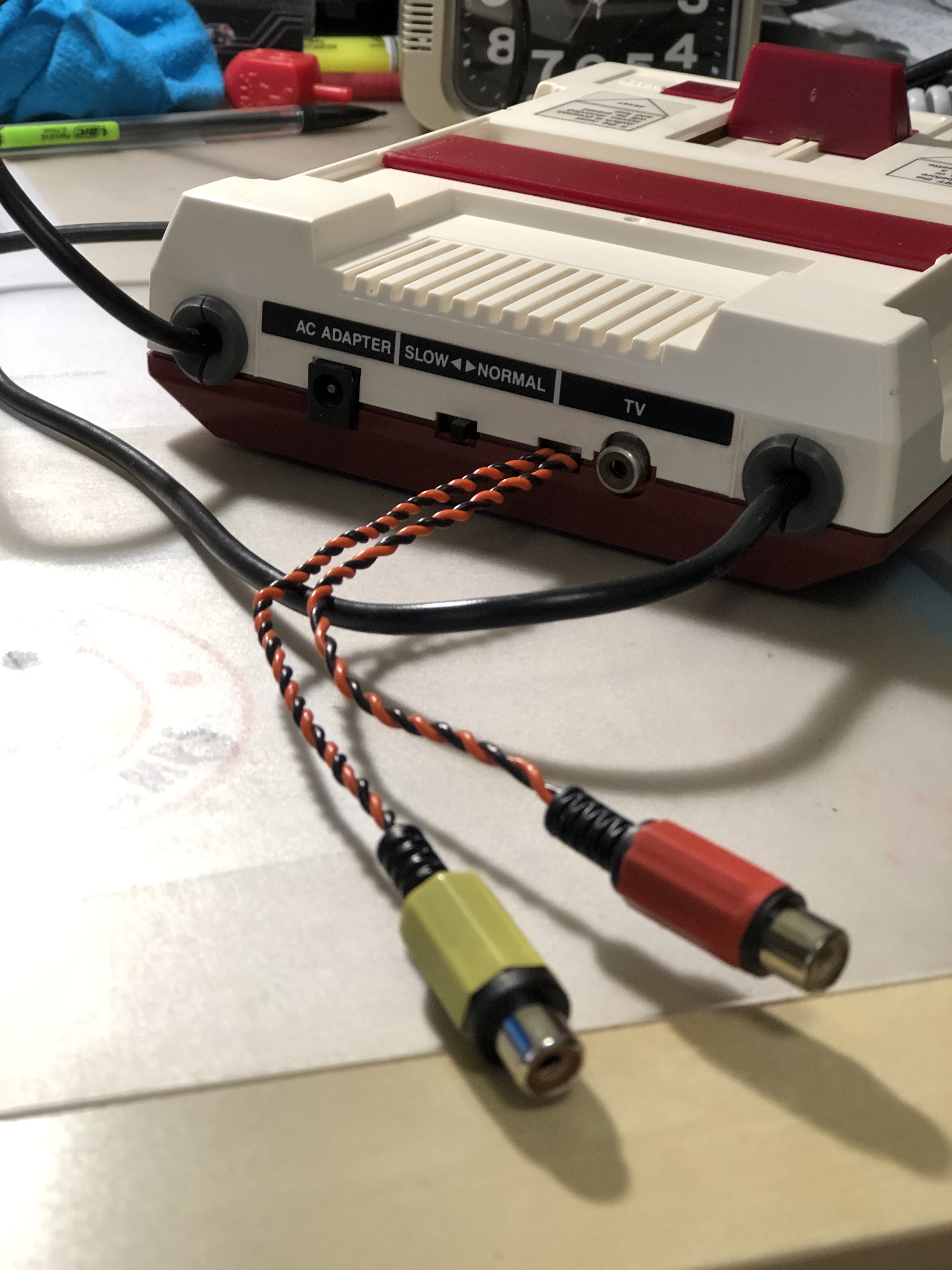 IMG_3682.jpg [ 1.59 MiB | Viewed 788 times ]
Attachment:
File comment: Bottom of the board, where the circuit is attached to the PPU.
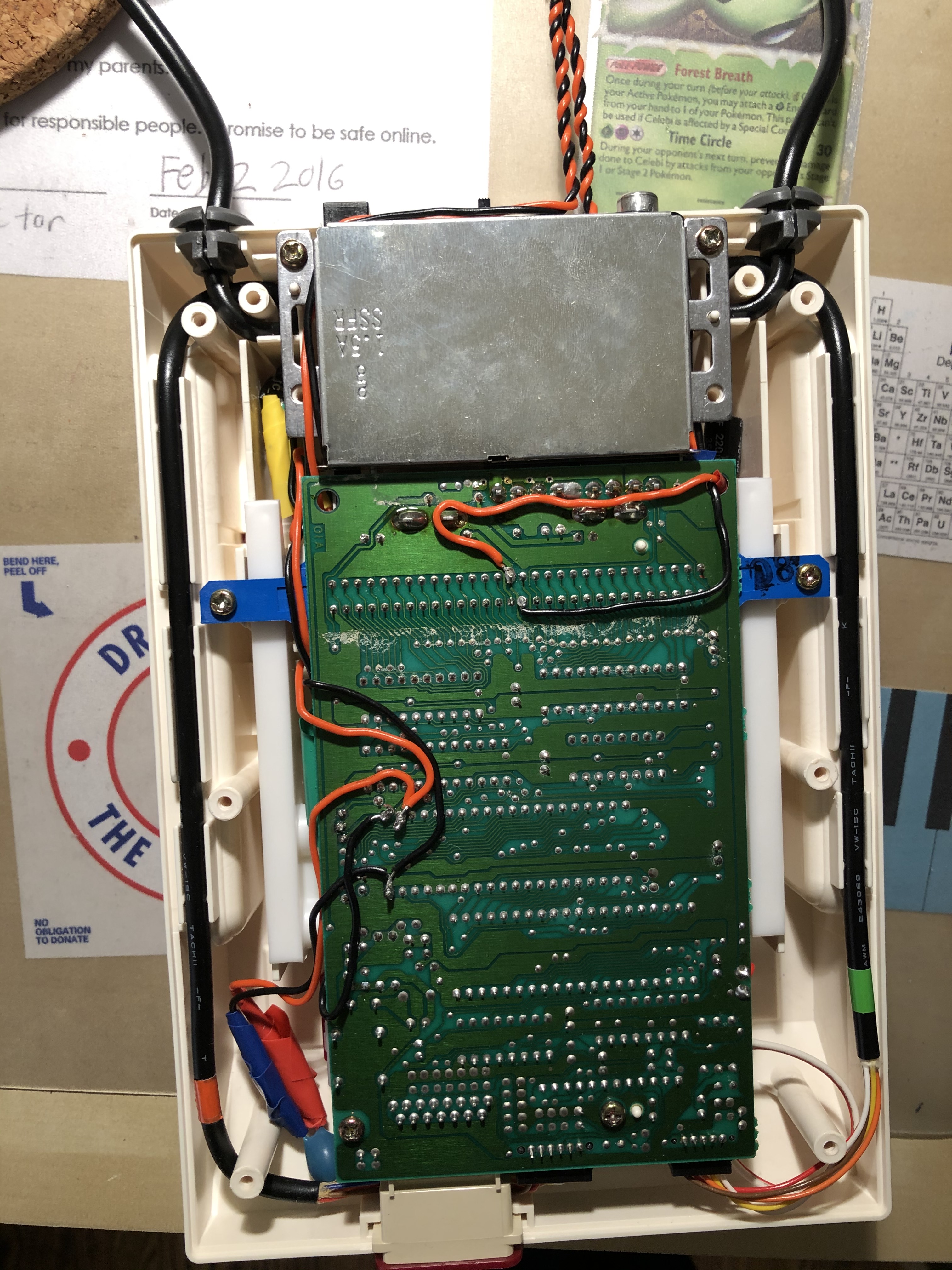 IMG_3683.jpg [ 2.2 MiB | Viewed 788 times ]
I had trouble soldering the components to the pins at the top lol, so I just added wire in order to solder to the bottom. Notice how the electrolytic capacitors for both video and audio are tucked into negative space just out of clearance of the cartridge eject mechanism. As well, there cannot be anything along the long part of the cartridge eject because it sits on an extruding part of the Famicom's case bottom. The tantalum is also placed into negative space as it won't fit directly on the bottom of the board.
Attachment:
File comment: Front of the board.
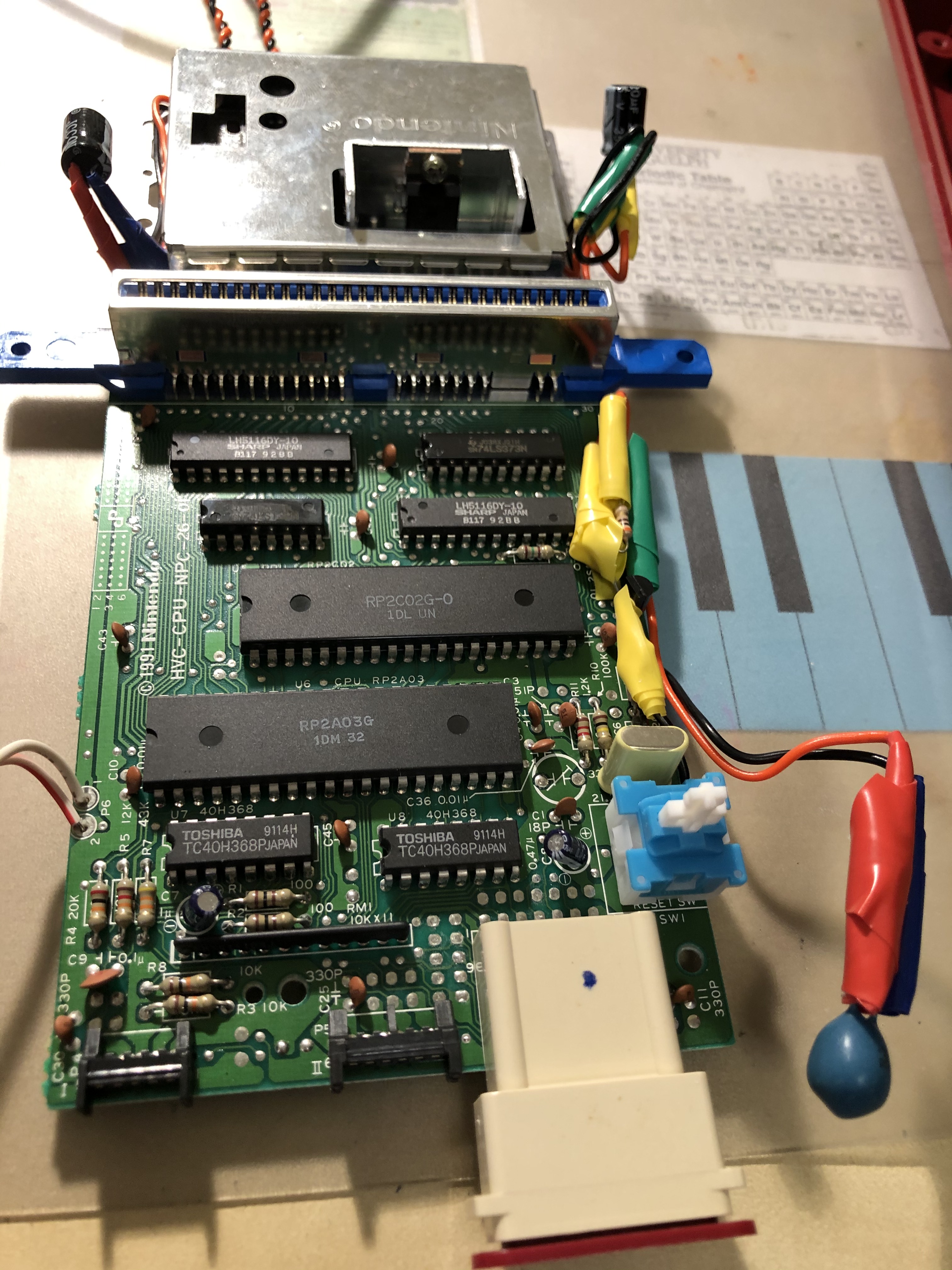 IMG_3684.jpg [ 2.02 MiB | Viewed 788 times ]
Here's two games I tested with, using a 28" Sharp flatscreen LCD.
Attachment:
File comment: Tetris Level 7. Looks fine.
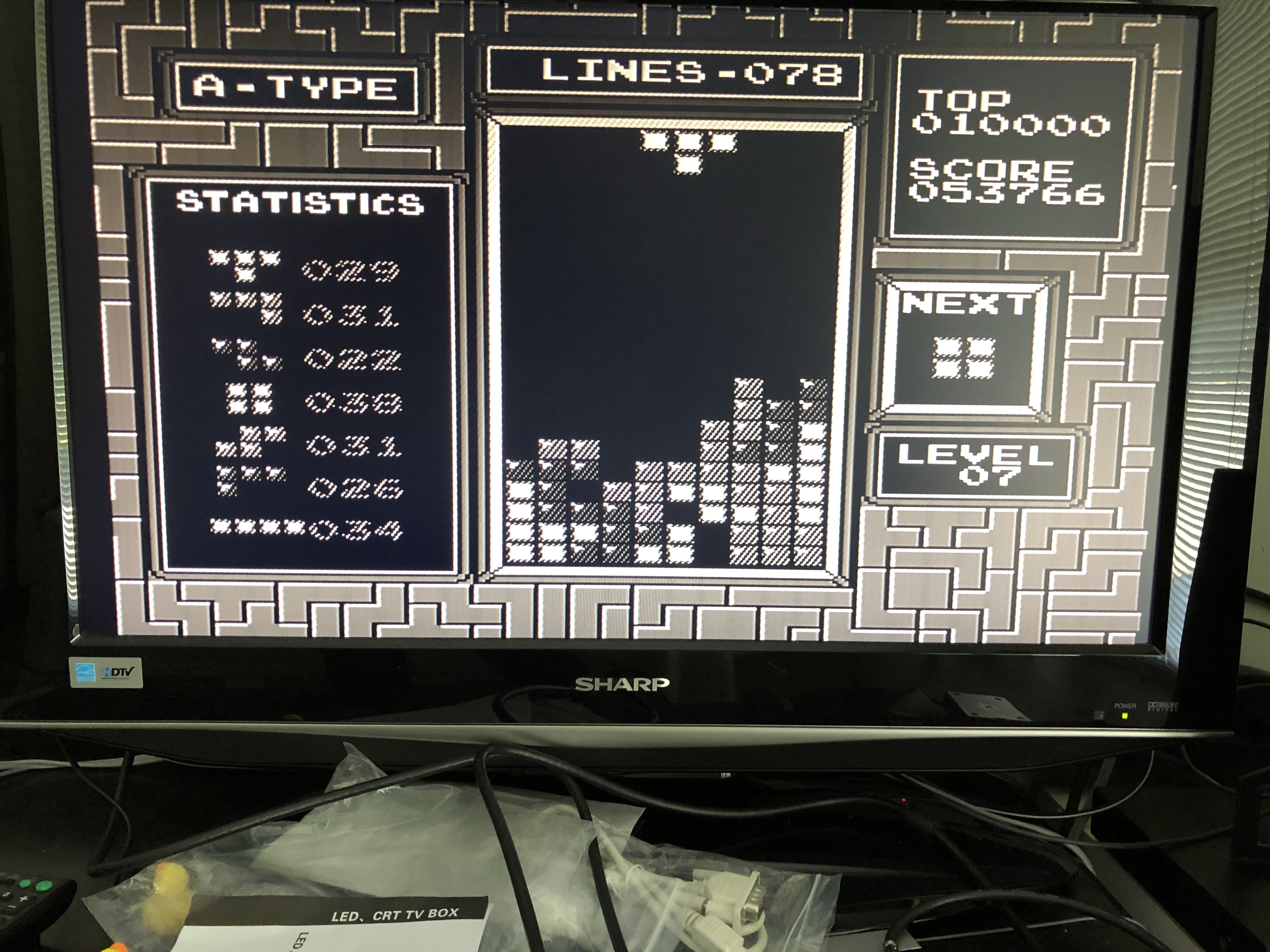 IMG_3687.jpg [ 2.6 MiB | Viewed 788 times ]
Whenever I got to this level in Tetris while I was using the RF, many of those darker pieces would just blend with the background because of the quality of that output, but on the AV I can actually tell those dark pieces apart (and therefore not have major anxiety playing that part lol)
Attachment:
File comment: Super Mario USA (aka Super Mario 2)
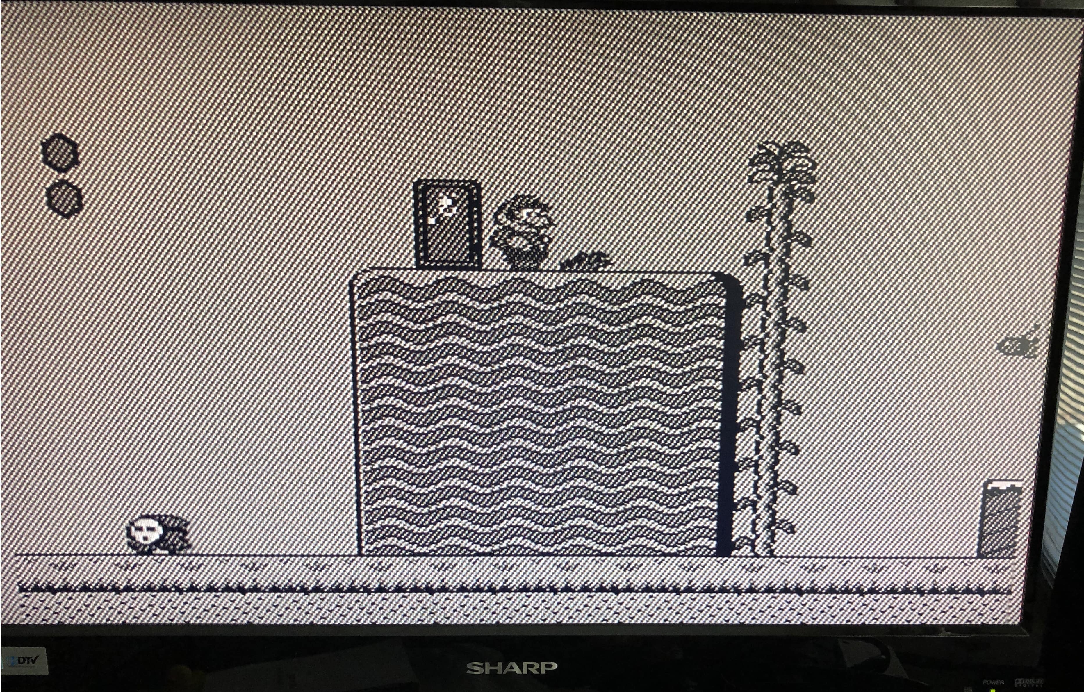 IMG_3689-min.jpg [ 1.73 MiB | Viewed 788 times ]
Honestly I don't know what's up with those diagonal lines. Probably something to do with the fact that my Famicom is in monochrome?
I know it's a bit off-topic, but if anyone has suggestions on what I can do to fix the monochrome please help me
Adjust the clock crystal for the famicom.
... Why is the trim cap missing?
Attachment:
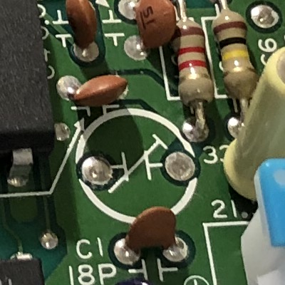 crop_IMG_3684.jpg [ 50.52 KiB | Viewed 778 times ]
TVs won't decode NTSC color unless the frequency is within 3ppm of correct (officially. Real TVs are probably more tolerant); your Famicom is probably running several hundred ppm too fast due to the missing trimcap.
lidnariq wrote:
Adjust the clock crystal for the famicom.
... Why is the trim cap missing?
Attachment:
crop_IMG_3684.jpg
TVs won't decode NTSC color unless the frequency is within 3ppm of correct (officially. Real TVs are probably more tolerant); your Famicom is probably running several hundred ppm too fast due to the missing trimcap.
I'm going to start a new thread, so that this thread doesn't get derailed, because my post will be more about Hong Kong Famicoms than about AV modding (now that I've completed this circuit successfully). Let's continue the discussion
there.