
I got this one from MLX quite long time ago. I was trying to analyze it but the mapper seems to be strange and I did not get satisfying results.
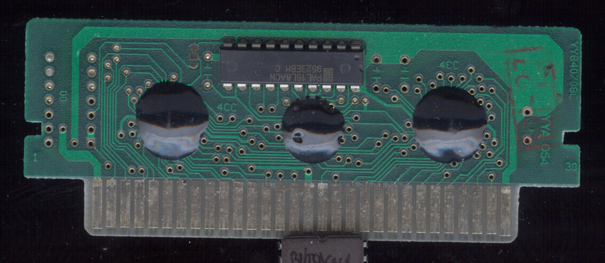
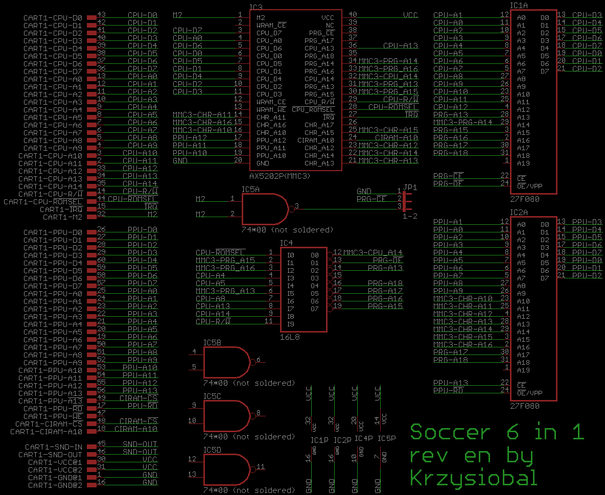
It has 512kB PRG + 512kB CHR on-board, blob MMC3, PAL16L8, unpopulated 7400 and consists of the following games:
Code:
Game [original title] | MPR | PRG | CHR
-----------------------------------------------------------------+-------+------+-----
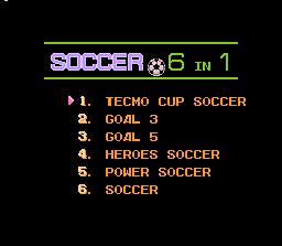
1. Tecmo Cup - Soccer Game | MMC1 | 128k | 128k
2. Goal 3 [Kunio Kun no Nekketsu Soccer League hack] | MMC3 | 128k | 128k
3. Goal 5 Soccer (Unl) | MMC3 | 64k | 64k
4. Heroes Soccer [Nekketsu Koukou Dodgeball Bu - Soccer Hen (J)] | MMC3 | 128k | 128k
5. Power Soccer | CNROM | 32k | 32k
6. Soccer | NROM | 32k | 8k
-----------------------------------------------------------------+-------+------+-----
1. Tecmo Cup - Soccer Game | MMC1 | 128k | 128k
2. Goal 3 [Kunio Kun no Nekketsu Soccer League hack] | MMC3 | 128k | 128k
3. Goal 5 Soccer (Unl) | MMC3 | 64k | 64k
4. Heroes Soccer [Nekketsu Koukou Dodgeball Bu - Soccer Hen (J)] | MMC3 | 128k | 128k
5. Power Soccer | CNROM | 32k | 32k
6. Soccer | NROM | 32k | 8k
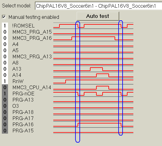
* PRG-ROM's A13/A15/A16/A17/A18 and CHR-ROMS's A17/A18 are controlled by PAL
* PRG-ROM's A14 and CHR-ROM's A10-A16 are controlled by MMC3
* MMC3's_CPU_A14 is controlled by PAL which can change its behavior in certain mode
(for example - map something other than -2/-1 at $c000-$ffff)
I desoldered the PAL for analysis and dumped the contents of the ROM, directly
providing values for the PRG address lines, so the dump is complete. However I am
unable to find out how exactly the mapper works.
https://anonymousfiles.io/r0sym6ml/
Here are my notes:
Code:
PAL16L8
,---v---.
CPU-!ROMSEL -> |01 20| -- VCC
MMC3-PRG-A15 -> |02 19| -> PRG-A15
MMC3-PRG-A16 -> |03 18| -> PRG-A16
CPU-A4 -> |04 17| -> PRG-A17
CPU-A5 -> |05 16| -> PRG-A18
MMC3-PRG-A13 -> |06 15| -> O3 (fedback)
CPU-A8 -> |07 14| -> PRG-A13
CPU-A13 -> |08 13| -> PRG-!OE
CPU-A14 -> |09 12| -> MMC3-CPU-A14
GND -- |10 11| <- CPU-R/!W
+-------+
Analyzing combinatorial outputs:
PRG_nOE <= (!CPU_A13 & CPU_nROMSEL) | (!CPU_A14 & CPU_nROMSEL) | (!CPU_RnW);
shows that PRG-ROM is enabled also at $6000 (no single game needs that,
but the menu code is ran from that region).
Because PAL does not take M2 into account so the PRG-/OE can be enabled when
M2 is low (when CPU address is not valid), ROM-/CE was meant to be inverted M2
(solder jumper selects between /ME and GND and because there is no 7400, it is choosen to be GND)
Analyzing latched outputs:
O3 <= '0' when (!CPU_RnW & !CPU_A13 & CPU_A8 & !CPU_nROMSEL) else
'1' when (!CPU_RnW & CPU_A13 & CPU_A8 & !CPU_nROMSEL);
PRG_A17 <= '0' when (!CPU_RnW & CPU_A8 & !CPU_A4 & !CPU_nROMSEL) else
'1' when (!CPU_RnW & CPU_A8 & CPU_A4 & !CPU_nROMSEL);
PRG_A18 <= '0' when (!CPU_RnW & CPU_A8 & !CPU_A5 & !CPU_nROMSEL) else
'1' when (!CPU_RnW & CPU_A8 & CPU_A5 & !CPU_nROMSEL);
shows that there are 3 bits being lathed, whose address overlap with mirrors
of the the regular MMC3 registers
fedc ba98 7654 3210
A~[1.u. ...1 ..vw ....]
| ||
| |+-- PRG-A17 = CHR-A17
| +--- PRG-A18 = CHR-A18
+------------- O3
---
Analyzing combinatorial outputs with feedback (PRG_A13)
PRG_A13 = (PRG_A17 & PRG_A18 & CPU_A13) |
(!PRG_A18 & MMC3_PRG_A13) |
(!PRG_A17 & MMC3_PRG_A13);
PRG_A18 PRG_A17 | PRG_A13
----------------+---------------
0 0 | = MMC_PRG_A13
0 1 | = MMC_PRG_A13
1 0 | = MMC_PRG_A13
1 1 | = CPU_A13
---
Analyzing combinatorial outputs with feedback (PRG_A14)
MMC3_CPU_A14 = (PRG_A17 & PRG_A18 & CPU_RnW & !CPU_A14 & !CPU_nROMSEL) |
(!CPU_RnW & CPU_A14) |
(!PRG_A18 & CPU_A14) |
(!PRG_A17 & CPU_A14) |
(CPU_A14 & CPU_nROMSEL);
shows that selection of outer bank (PRG_A18/PRG_A17) affects MMC3 behaviour:
behaviour for writes:
MMC3_CPU_A14 = CPU_A14 (that is all MMC3 regs are written normally)
behaviour for reads:
PRG_A18 PRG_A17 CPU_A14 CPU_!ROMSEL | MMC3_CPU_A14
------------------------------------+---------------
1 1 0 0 | 1
1 1 1 0 | 0
----------- otherwise ------------- | CPU_A14
so the standard MMC3 mapping
| $8000 | $a000 | $c000 | $e000 |
| $8001.R6 | $8001.R7 | -2 | -1 | (when $8000.6=0)
| -2 | $8001.R7 | $8001.R6 | -1 | (when $8000.6=1)
becomes
| -2 | -1 | $8001.R6 | $8001.R7 | (when $8000.6=0)
| $8001.R6 | -1 | -2 | $8001.R7 | (when $8000.6=1)
I was not able to automatically check PRG_A15/PRG_A16 behavior so I analyzed them manually:
Formula for PRG_A15
PRG_A18 PRG_A17 O3 |$6000 |$8000 |$a000 |$c000 |$e000 |
0 0 0 |0 |0 |0 |0 |0 |
0 0 1 |1 |1 |1 |1 |1 |
-------else------- |MMC3_PRG_A15|MMC3_PRG_A15|MMC3_PRG_A15|MMC3_PRG_A15|MMC3_PRG_A15|
(So O3 seems to be PRG_A15 when PRG_A18=0 and PRG_A17=0)
---
Formula for PRG_A16
PRG_A18 PRG_A17 O3 |$6000 |$8000 |$a000 |$c000 |$e000 |
0 0 * |- |MMC3_PRG_A16|MMC3_PRG_A16|- |- | (only reads latches)
------else-------- |MMC3_PRG_A16|MMC3_PRG_A16|MMC3_PRG_A16|MMC3_PRG_A16|MMC3_PRG_A16|
This is the only thing that I do not understand - the value of PAL output (PRG_A16)
is in fact a latch, which latches the MMC3_PRG_A16 when CPU_A14=0 and /ROMSEL edge falls
(when read from $8000-$bfff occurs) - I don't even know how to emulate that.
* All latched bits are set to 0 on powerup