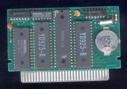
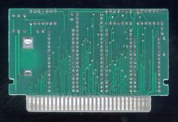
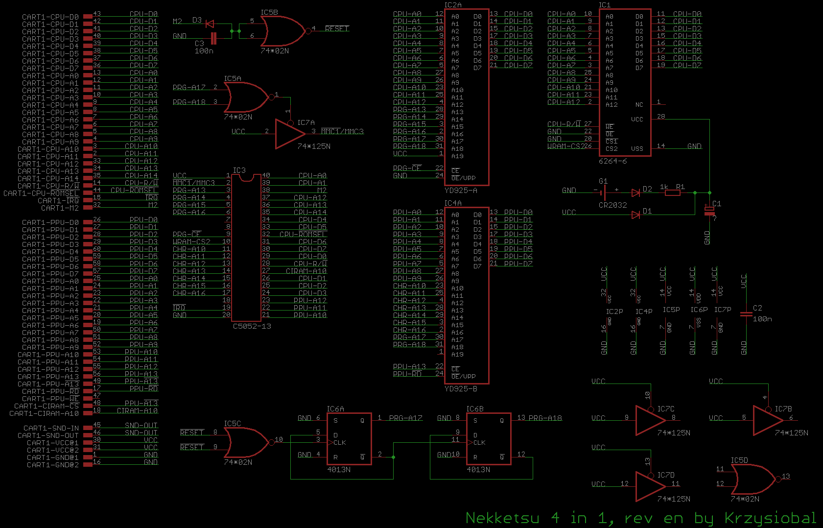
This reset-baset cartridge consists of 4 games and uses mysterious DIP40 "C5052-13" chip (and a battery backup which is rare for pirate games).

At first I thought it is MMC3 clone, but when I dumped the games, one of them turned out to be MMC1:
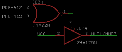
Depending on the pin 2, it switches its functionality between MMC1 (disconnected) and MMC3 (VCC).
The connection was unclear to me:
* they used additional 74125 buffer just to invert the signal (three other 74125's gates are unused), but there was still one 7402 NOR unused that could be utilized for that purpose.
* the output of 74125 is not pulled down which causes the signal to be at 2.5V when in MMC1 mode
* CPU-A1 and CPU-A12 are wired into mapper but neither MMC1 nor MMC3 needs it
When in MMC1 mode, PRG A18 is at GND and so does CHR A17.
Then I tried pulling pin 2 to ground (using 100R resistor for safety) and it seems to go into third mode. I thought it might be VRC2 or VRC4.
* Writing $00/$01/$02/$03 to $9000/$9001/$9002/$9003 switches between V and H mirroring (so it seemed to be VRC2 as VRC4 has also 0/1 mode), but
* Writing to any of $X00Y where X=8/9/a/b/c/d/e/f and Y=0/1/2/3 does not seem to alter PRG bank
* Writing to $b000/b001 (and $b002/$b003) manipulates CHR bank at $400.
* When in MMC3/MMC1 mode - WRAM at $6000-$7fff is enabled and when in this semi-VRC mode, it is disabled
Either the VRC2 mode is broken, or this is not VRC chip.


At first I thought it is MMC3 clone, but when I dumped the games, one of them turned out to be MMC1:
Code:
Downtown - Nekketsu Koushin Kyoku - Soreyuke Dai Undoukai (J) | MMC3
Downtown Special - Kunio Kun no Jidaigeki Dayo Zenin Shuugou! (J) | MMC3 + WRAM + battery backup
Nekketsu Kakutou Densetsu (J) | MMC3
Nekketsu Koukou Dodgeball Bu (J) | MMC1
Downtown Special - Kunio Kun no Jidaigeki Dayo Zenin Shuugou! (J) | MMC3 + WRAM + battery backup
Nekketsu Kakutou Densetsu (J) | MMC3
Nekketsu Koukou Dodgeball Bu (J) | MMC1
Depending on the pin 2, it switches its functionality between MMC1 (disconnected) and MMC3 (VCC).
The connection was unclear to me:
* they used additional 74125 buffer just to invert the signal (three other 74125's gates are unused), but there was still one 7402 NOR unused that could be utilized for that purpose.
* the output of 74125 is not pulled down which causes the signal to be at 2.5V when in MMC1 mode
* CPU-A1 and CPU-A12 are wired into mapper but neither MMC1 nor MMC3 needs it
When in MMC1 mode, PRG A18 is at GND and so does CHR A17.
Code:
.--\/--.
+5V -- |01 40| <- CPU A0
mode -> |02 39| <- CPU A1
PRG A13 <- |03 38| <- M2
PRG A14 <- |04 37| <- CPU A12
PRG A15 <- |05 36| <- CPU A13
PRG A16 <- |06 35| <- CPU A14
PRG A17 <- |07 34| <- CPU D4
PRG A18 <- |08 33| <- CPU D5
PRG /CE <- |09 32| <- CPU /ROMSEL
WRAM +CE <- |10 31| <- CPU D6
CHR A10 <- |11 30| <- CPU D7
CHR A11 <- |12 29| <- CPU D0
CHR A12 <- |13 28| <- CPU R/!W
CHR A13 <- |14 27| -> CIRAM A10
CHR A14 <- |15 26| <- CPU D1
CHR A15 <- |16 25| <- CPU D2
CHR A16 <- |17 24| <- CPU D3
CHR A17 <- |18 23| -> PPU A12
/IRQ <- |19 22| -> PPU A11
GND -- |20 21| -> PPU A10
`------'
C5052-13
Then I tried pulling pin 2 to ground (using 100R resistor for safety) and it seems to go into third mode. I thought it might be VRC2 or VRC4.
* Writing $00/$01/$02/$03 to $9000/$9001/$9002/$9003 switches between V and H mirroring (so it seemed to be VRC2 as VRC4 has also 0/1 mode), but
* Writing to any of $X00Y where X=8/9/a/b/c/d/e/f and Y=0/1/2/3 does not seem to alter PRG bank
* Writing to $b000/b001 (and $b002/$b003) manipulates CHR bank at $400.
* When in MMC3/MMC1 mode - WRAM at $6000-$7fff is enabled and when in this semi-VRC mode, it is disabled
Either the VRC2 mode is broken, or this is not VRC chip.