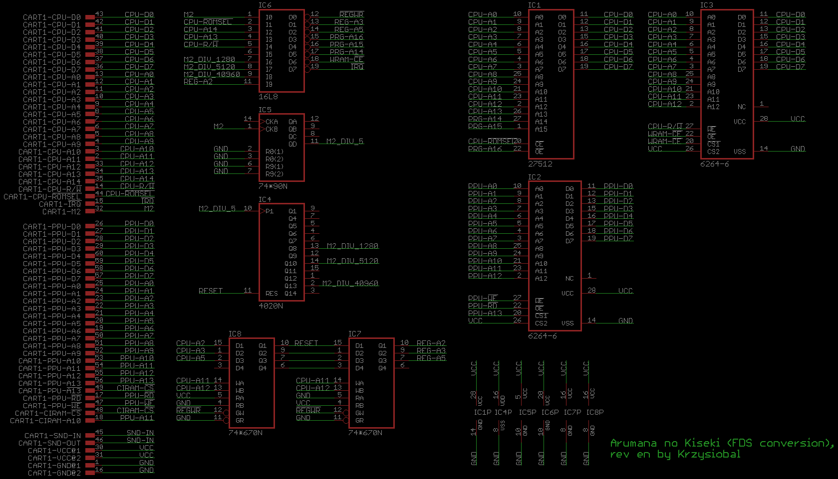
Code:
PRG:
ROM 128 kB
RAM 8 kB
CHR:
RAM 8 kB
Bus conflicts: yes
Mirroring: hardwired to H
$4800: Register #1 (mask $F800)
fedcba9876543210
A~[01001.....A.BC..]
| ||
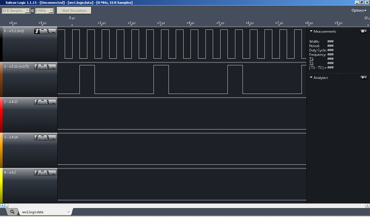
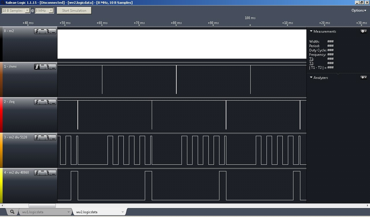
| |+-- IRQ/Counter:
| || 0=IRQs are enabled, counter clocks falling edges of M2.
| || After 23680 edges (40960+5120+1280)/2, IRQ is fired and will be
| || self-acked after another 1280/2 edges (this game seems to use self-acking!)
| || 1=pending IRQ is acknowledged, IRQs are disabled, counter is halted and set to 0
+-++-- used as latch for register #2
$5000: Register #2 (mask $f800)
fedcba9876543210
A~[01010...........] DEF
|||
+++- ABC from $4800 is stored into DEF. DEF xor 0b101 will be used as bank at $8000
Notes:
* All bits in both registers are set to 1 on powerup (thats how 74670 behaves on powerup)
* To write V to register #2, set ABC from register #1 to V and then write any value to any address range of register #2
Memory map:
$6000 $8000 $c000
RAM ROM ROM
DEF 011
xor
0b101
PAL equations:
nREGWR = (!M2) | (!CPU_nROMSEL) | (!CPU_A14) | (CPU_RnW) | (CPU_A13);
PRG_A16 = (!REG_A5 & !CPU_A14);
PRG_A15 = (REG_A3) | (CPU_A14);
PRG_A14 = (!REG_A2) | (CPU_A14);
WRAM_nCE = (!M2) | (!CPU_nROMSEL) | (!CPU_A14) | (!CPU_A13);
nIRQ = (!M2_DIV1280) | (!M2_DIV5120) | (!M2_DIV40960);
ROM 128 kB
RAM 8 kB
CHR:
RAM 8 kB
Bus conflicts: yes
Mirroring: hardwired to H
$4800: Register #1 (mask $F800)
fedcba9876543210
A~[01001.....A.BC..]
| ||
| |+-- IRQ/Counter:
| || 0=IRQs are enabled, counter clocks falling edges of M2.
| || After 23680 edges (40960+5120+1280)/2, IRQ is fired and will be
| || self-acked after another 1280/2 edges (this game seems to use self-acking!)
| || 1=pending IRQ is acknowledged, IRQs are disabled, counter is halted and set to 0
+-++-- used as latch for register #2
$5000: Register #2 (mask $f800)
fedcba9876543210
A~[01010...........] DEF
|||
+++- ABC from $4800 is stored into DEF. DEF xor 0b101 will be used as bank at $8000
Notes:
* All bits in both registers are set to 1 on powerup (thats how 74670 behaves on powerup)
* To write V to register #2, set ABC from register #1 to V and then write any value to any address range of register #2
Memory map:
$6000 $8000 $c000
RAM ROM ROM
DEF 011
xor
0b101
PAL equations:
nREGWR = (!M2) | (!CPU_nROMSEL) | (!CPU_A14) | (CPU_RnW) | (CPU_A13);
PRG_A16 = (!REG_A5 & !CPU_A14);
PRG_A15 = (REG_A3) | (CPU_A14);
PRG_A14 = (!REG_A2) | (CPU_A14);
WRAM_nCE = (!M2) | (!CPU_nROMSEL) | (!CPU_A14) | (!CPU_A13);
nIRQ = (!M2_DIV1280) | (!M2_DIV5120) | (!M2_DIV40960);

https://gofile.io/?c=ejR0XP