This is a pretty simple question. What is the threshold voltage for what the 2A03 sees as a logic high coming in?
NMOS technology (which is fully compatible with CMOS I guess)
Bregalad wrote:
NMOS technology (which is fully compatible with CMOS I guess)
Is 3.3V logic enough to drive it?
Might work.......definitly not "correct though" stick to 5v for nes.
Mmh... You'd definitely want to adds pull-up resistors and/or to test the thing extensively.
I have enough trouble making my 5V board working. The possible sources of error are so numerous that it's a headache (power filtering, good electrical connexion, problem with delays, problem with contacts, solder short-circuit, via touching another componant or solder, etc...).
You don't want to intentionally add more possible errors.
Ya but then you'd have problems with possible revisions. With some nesses working some dont.....just stick to 5v
I was hoping it would be CMOS/TTL compatible. It would save some parts/hassle
I haven't had any problems driving the 2A03 with 5V CMOS, but that's the most ideal possible case.
Looks like it'll have to be open-drain or buffered circuitry.
I haven't had any problems driving the 2A03 with 5V CMOS, but that's the most ideal possible case.
Looks like it'll have to be open-drain or buffered circuitry.
Has anyone ever seen a 2A03 datasheet? I'd love to have one even in Japanese.
HMOS is an improved version of NMOS, isn't it? I noticed the HMOS SID chips that I have are rated for 2V being logic high with a 5V power supply. How different is NMOS?
HMOS is an improved version of NMOS, isn't it? I noticed the HMOS SID chips that I have are rated for 2V being logic high with a 5V power supply. How different is NMOS?
I wasn't aware of HMOS, but according to Wikipedia it's also known as "depletion-load NMOS". The 2 6500 datasheets I just looked at (Rockwell and Commodore) both say it's "N-channel, silicon-gate, depletion-load technology".
2A03 is a clone (excluding the patented BCD mode), I'd assume it's made on the same way..? If that's true, maybe this is accurate enough:
http://www.zimmers.net/anonftp/pub/cbm/ ... 50x-15.gif
2A03 is a clone (excluding the patented BCD mode), I'd assume it's made on the same way..? If that's true, maybe this is accurate enough:
http://www.zimmers.net/anonftp/pub/cbm/ ... 50x-15.gif
That sounds promising. I'll give it a test soon and see what magic happens.
Let us know how it goes. There is a lot of stuff that is 3V.
I wonder if the PPU would be the same?
I wonder if the PPU would be the same?
Wasn't part of the issue with the PowerPAK and the FPGA needed being expensive cause it was an older 5V type? Or am I mistaken?
MottZilla wrote:
Wasn't part of the issue with the PowerPAK and the FPGA needed being expensive cause it was an older 5V type? Or am I mistaken?
Yeah, 5V parts tend to be less available and more expensive than 3V equivalents (if equivalents exist, often they don't, and maybe never exist for new architectures).
I would think the NES can read a 3V signal is being '1', but you still won't be able to use a 5V output from the NES on a 3V system. So it's just a possible optimization, for some simpler cases.
MottZilla wrote:
Wasn't part of the issue with the PowerPAK and the FPGA needed being expensive cause it was an older 5V type? Or am I mistaken?
I'm looking at using some CPLDs that have 3.3V outputs and 5V tolerant inputs. As long as the 2A03 can see 3.3V as logic high then there is no problem with communication.
FPGAs are a bit of a different beast. Even 3.3V can be too much for some modern FPGAs. In that case you need a special FPGA or level shifting circuitry so that the 5V from the NES doesn't cause damage.
Can't you just put a resistor in, so that the voltage is reduced to 3.3V via the input protection diodes and the current limited by the resistor? Slew rate will be degraded in both directions, of course.
But then you'd somehow have to get signals going back to the NES up above the threshold somehow.
Isn't the minimum high output of the 3.3V part greater than the minimum high input for the 2A03? Heh, or you could float the 3.3V part above ground...
Memblers wrote:
Let us know how it goes. There is a lot of stuff that is 3V.
I wonder if the PPU would be the same?
I wonder if the PPU would be the same?
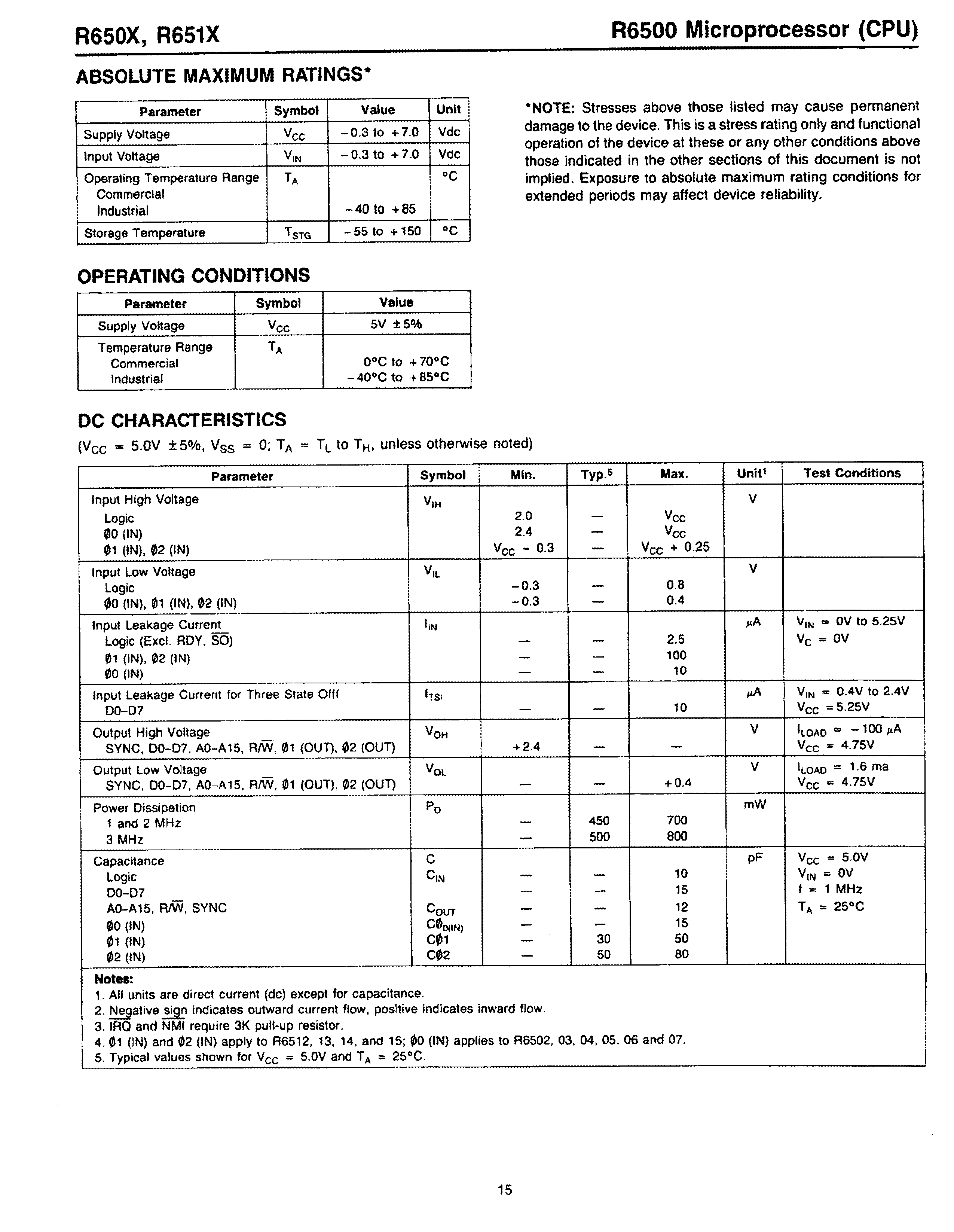
I did a pseudo-scientific test today. It seems to be working!
I made up two versions of the same circuit. One used several logic gates and flip flops, and the other used a CPLD with the same parts coded in Verilog. I looked at both with my logic analyzer. If the 3.3V signals weren't enough to trigger logic on the 2A03, the chip would've screeched to a halt. Instead, it kept running as long as I checked it (a few times over a couple hours).
Here is the discrete logic version:
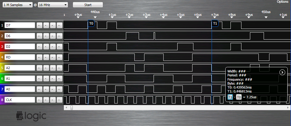
...and here is the 3.3V CPLD version:
They are running at different speeds intentionally. The CPLD version is clocked at 20MHz, and the glue logic version is running at NES speed.
I'm not sure why there is such a difference on the address pins when R/W goes low, but it doesn't seem to affect performance. I don't really know why the processor is trying to write at all, but it comes up in both circuits.
(off topic) Which logic analyzer is that? The UI looks pretty!
It's a Saleae Logic. It has terrible specs, but it looks really pretty and is great for simple data logging over long spans of time.
skrasms wrote:
It's a Saleae Logic. It has terrible specs, but it looks really pretty and is great for simple data logging over long spans of time.
whoa! it works on Linux and OSX too, but only 8 inputs and 24MHz? Know a better one that might work on a machine I own (I use Linux and OSX so either one). It would be nice if I could do more like 24 inputs and capture writes to mapper registers for example.
I do have a use for the Saleae at work just for doing I2C, SPI, rs232 and MMC/SD, so I'm tempted to get one anyways.
(sorry to hijack the thread)
Thanks for confirming that. I've suspected it would work. I figured that'd be kinda wrong for it to be the regular NMOS since many (most?) carts used CMOS parts entirely and Nintendo's hardware seems to be pretty much "by the book". (though I suppose it is "the book" for me, since that's what I've learned based on, heheh)
Now I wonder if the PPU is the same, in light of this though, I'd say almost certainly. Now, if only more parts had 5V tolerant inputs.
Now I wonder if the PPU is the same, in light of this though, I'd say almost certainly. Now, if only more parts had 5V tolerant inputs.
Jon wrote:
whoa! it works on Linux and OSX too, but only 8 inputs and 24MHz? Know a better one that might work on a machine I own (I use Linux and OSX so either one). It would be nice if I could do more like 24 inputs and capture writes to mapper registers for example.
I do have a use for the Saleae at work just for doing I2C, SPI, rs232 and MMC/SD, so I'm tempted to get one anyways.
(sorry to hijack the thread)
I'm still looking for something affordable that has 32 channels, 200+ MHz, and any kind of memory buffer. It seems like the only real solutions for that are closer to $1000.
I almost bought the LA1034 LogicPort by Intronix, but I did the calculations and it can only record about 20 microseconds of a 100MHz clock.
Since you can use CPLD, why not make your own logic analyzer with a synchronous SRAM? For ~$8 you can get a 200MHz 4M one (128K x 36 bit) in a TQFP100 package from Digikey no less. This is what I plan to do someday when I finally get around to projects needing a real LA.
skrasms wrote:
I'm still looking for something affordable that has 32 channels, 200+ MHz, and any kind of memory buffer. It seems like the only real solutions for that are closer to $1000.
I almost bought the LA1034 LogicPort by Intronix, but I did the calculations and it can only record about 20 microseconds of a 100MHz clock.
Byte Paradigm started putting 8MB buffers in all their portable LAs. I haven't tried them, but they looked pretty impressive for around $800-1200 when I checked them out at the recent ESC tradeshow. But I think they are only able to sample 16-bit I/O.
Also interesting is the CircuitGear oscope which can sample 8-bits and also generate arbitrary wave forms. For around $180 it's more in my price range, but then it's even slower than the Saleae.
Is it really possible to cheaply make a LA out of a CPLD some SRAM and maybe a micro to provide USB access to the buffer? anything 24-bits or more for under $500 would suit me at almost any speed! I'll even write the USB drivers myself if I have to.
Jon wrote:
Is it really possible to cheaply make a LA out of a CPLD some SRAM and maybe a micro to provide USB access to the buffer? anything 24-bits or more for under $500 would suit me at almost any speed! I'll even write the USB drivers myself if I have to. :)
Sure, there's even a popular open project in Japan called ChameleonUSB which is basically a CPLD and Cypress MCU with IDC headers. It has a 100 MHz 32-channel Logic Analyzer attachment which is just a "PBSRAM" and protection resistors. The author also sells them, but getting one might be difficult without a friend in Japan. I believe it should come to under US$150 though if you chose to buy it with the 4M Logic Analyzer.
http://optimize.ath.cx/cusb/build2.html
http://optimize.ath.cx/cusb/logiana.html
http://www.teamknox.com/ChameleonNES/ChameleonNES.html
skrasms wrote:
I almost bought the LA1034 LogicPort by Intronix, but I did the calculations and it can only record about 20 microseconds of a 100MHz clock.
Thats the one I have, its good for the price. Limited recording is a problem but it does on device compression so if you have only a couple signals or they don't change often then you can get very long sampling. Software has pretty good edge/level triggering. Only having a USB cable is great too.
kyuusaku wrote:
Jon wrote:
Is it really possible to cheaply make a LA out of a CPLD some SRAM and maybe a micro to provide USB access to the buffer? anything 24-bits or more for under $500 would suit me at almost any speed! I'll even write the USB drivers myself if I have to.
Sure, there's even a popular open project in Japan called ChameleonUSB which is basically a CPLD and Cypress MCU with IDC headers. It has a 100 MHz 32-channel Logic Analyzer attachment which is just a "PBSRAM" and protection resistors. The author also sells them, but getting one might be difficult without a friend in Japan. I believe it should come to under US$150 though if you chose to buy it with the 4M Logic Analyzer.
http://optimize.ath.cx/cusb/build2.html
http://optimize.ath.cx/cusb/logiana.html
http://www.teamknox.com/ChameleonNES/ChameleonNES.html
You can get the ChameleonUSB on Yahoo Japan auctions too, I've also seen the logic analyzer pop up on there a few months ago. I got my ChameleonUSB from there.