I've been doing experiments with a 2A03 by itself for a synthesizer, and I do not understand some of the results. This test was conducted to see what happens on startup, when the chip first gets power and a clock. The setup is very simple: D7-D0 are tied through 10k ohm resistors to ground. When the 2A03 tries to read, it will always see 0x00. If any actual data comes out of the data bus, the 10k ohm resistors are simple loads to limit the current. NMI, IRQ, and RES are all tied to VCC for a logic high.
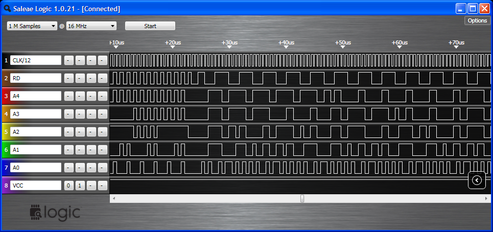
My logic analyzer is only 8 pins, so I went with VCC, RD/WR, CLK/12, A4-A0.
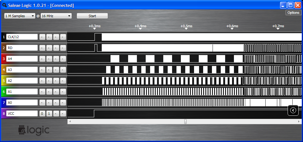
When the chip first gets power, it does a counting sequence of some kind before it starts.
Here is a close-up view
Eventually the processor tries to actually run a program. Since it is stuck reading 0x00, it gets a reset vector of 0x00 followed by BRK instructions that keep it looping.
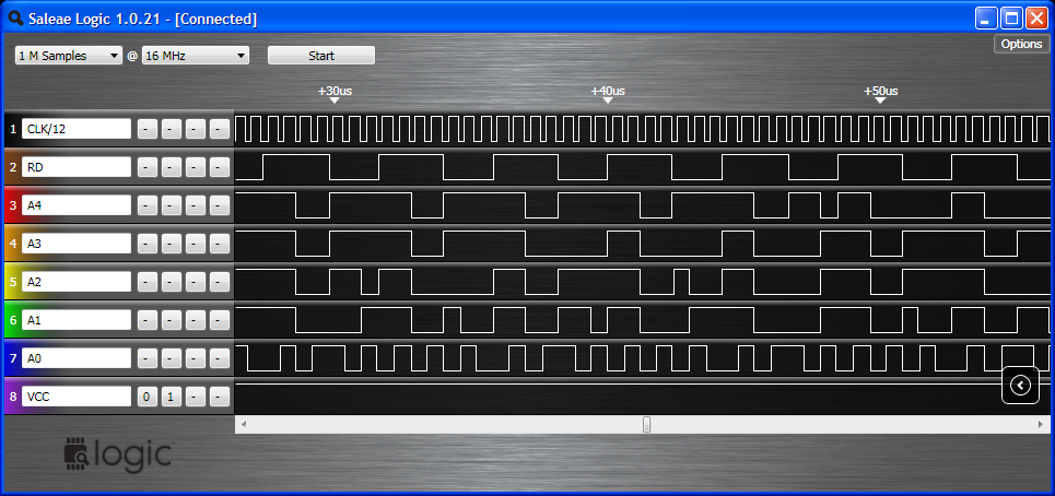
Here is a close-up view
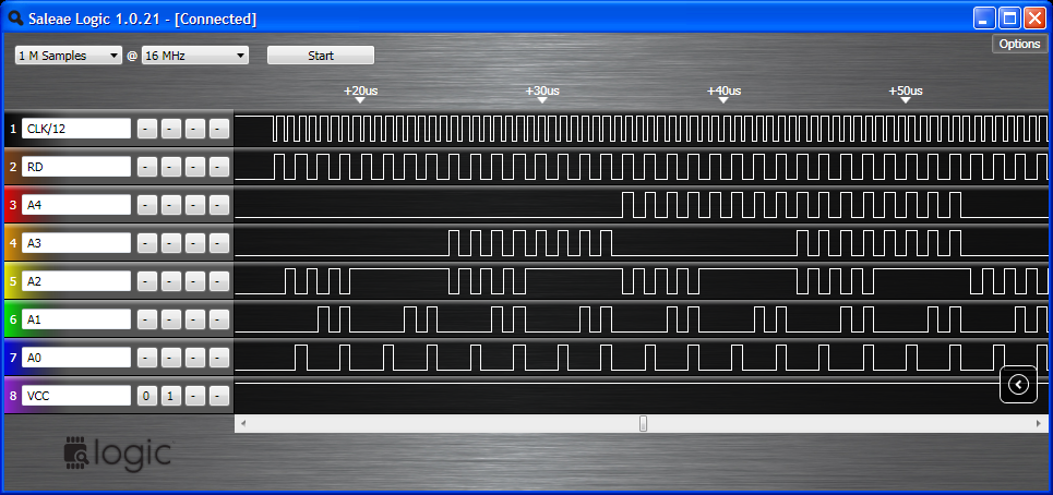
So what is the counting sequence at the beginning? It happens consistently every time, with A4 always having 8 bursts of logic toggles before the "program" starts.
I would also think that with this setup, the first thing I'd see on the address pins during execution would correspond with the reset vector location at 0xFFFC and 0xFFFD. That should be 11100 and 11101 on the five probed address bus pins while RD is high, but I don't see it happen. Am I missing something obvious?
Any help is appreciated
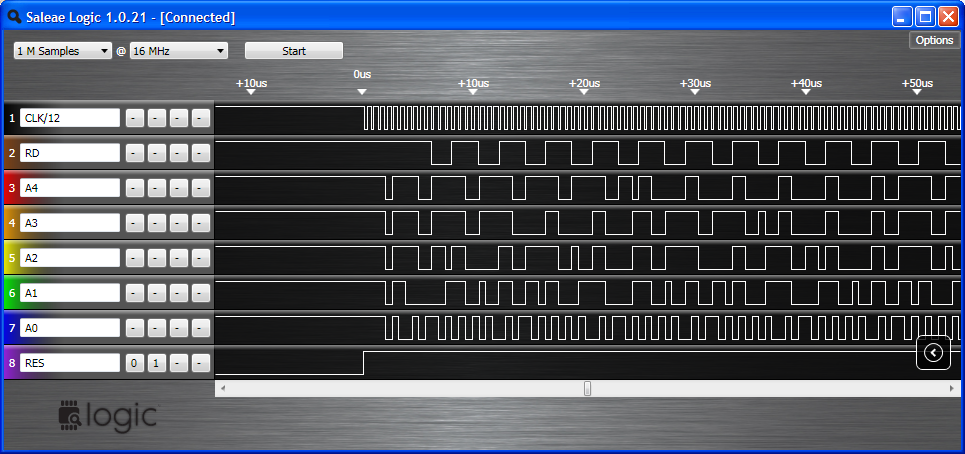
My logic analyzer is only 8 pins, so I went with VCC, RD/WR, CLK/12, A4-A0.
When the chip first gets power, it does a counting sequence of some kind before it starts.
Here is a close-up view
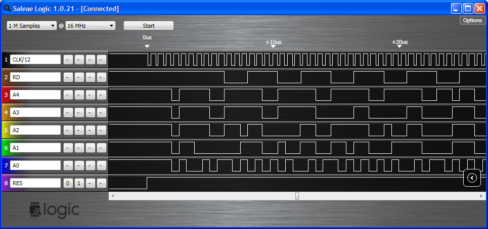
Eventually the processor tries to actually run a program. Since it is stuck reading 0x00, it gets a reset vector of 0x00 followed by BRK instructions that keep it looping.
Here is a close-up view
So what is the counting sequence at the beginning? It happens consistently every time, with A4 always having 8 bursts of logic toggles before the "program" starts.
I would also think that with this setup, the first thing I'd see on the address pins during execution would correspond with the reset vector location at 0xFFFC and 0xFFFD. That should be 11100 and 11101 on the five probed address bus pins while RD is high, but I don't see it happen. Am I missing something obvious?
Any help is appreciated