The PC10 version of Mike Tyson's Punch-Out has a record keeping feature for fastest times. I would like to have that feature on a regular NES cart.
I have established that I can put pc10 prg and chr on a punch out test cart and the game will run. i skipped ahead to the tyson fight and won, and then the game froze. I assume it's due to there not being anything in the wram space to update for record keeping.
donor issues:
no battery
no wram
I think I can work out the battery so let's skip that part for now.
How would I go about wiring wram to a punch out donor board? the wiki entry for mmc2 does not mention wram support, but based on what photos of the pc10 board I could find, it uses some version of the chip labeled as mmc2.
You can add WRAM to any mapper that doesn't already put something in $6000-$7FFF with
a 74HC20.
Apparently the PC10 Punchout module explicitly added battery-backed memory:
webarchive of gamersgraveyard.
As far as I can tell by
this picture, the skinny DIP on the top right (U2) is probably a RAM, either the shorter DIP in the middle (U7) or lower right (U8) is the RAM decoding IC (equivalent to a 74'20), and U6 is... um... that looks like it should be an 8-pin SPI or I2C EEPROM given its sticker, but that doesn't make sense. A battery controller would make more sense.
so using a 74-20, the inputs all connect back to the cart edge like so?
A = Phi2 (M2) pin 38
B = /ROMSEL (PRG /CE) pin 50
C = A14 pin 41
D = A13 pin 40
A13 and A14 are PRG right?
and for the 8K RAM it looks like
pin 20 (/CE1) = 7420 Y
pin 22 (/OE) = any GND
pin 26 (CE2) = M2 again ? (
see kevtris post)
pin 27 (R/W) = pin 14 (PRG R/W)
all the other A* and D* lines on the RAM can go to the respective pins on the PRG ROM?
FrankWDoom wrote:
pin 26 (CE2) = M2 again ? (
see kevtris post)
all the other A* and D* lines on the RAM can go to the respective pins on the PRG ROM?
You've already decoded all four signals so you may as well tie ce2 to Vcc. Kevtris was suggesting you would only have to decode PRG /CE, a14,13 if you connected m2 to ce2.
And yes, all address and data lines match up with PRG rom. Although if its easier for routing you REALLY only need to make sure an address line is connected to an a0-12 address line on the PRG rom, and similarly with data. You can mix any address pin with any address pin, and any data pin with any other data pin. And it'll all be the same.
Also one trick you can do is bend all the pins up and place the SRAM underneath the PRG rom on the BOTTOM of the pcb. Just make sure you keep the CE/we signals separate...
so if I run M2 for CE2, that would leave an input open on the 7420, which I wouldn't want to do, correct?. I would jump that pin over to the next input pin so it has proper hi/lo signals right?
Just so I'm sure I understand, we can mix up A lines (and D lines) and it's fine because as long as the signals are the same we always get the same byte back?
I think i'll try to mount the ram to the underside of the board first, since that saves a lot of effort cutting wires. It looks like it'll be tight in the cart but I'll give that a shot.
I guess now I wait for my 7420's to show up in the mail. Thanks for the help everyone.
FrankWDoom wrote:
so if I run M2 for CE2, that would leave an input open on the 7420, which I wouldn't want to do, correct?
There is no harm (although no benefit either) to having M2 on both the 7420 and the 6264. If you hadn't already bought them, I might suggest you try buying a 7410 (3-input NAND) instead. But yes, avoid floating inputs.
And yes, for a RAM you can completely scramble the A lines with other A lines, and D lines with other D lines. But the order for A12..A0 and D0..D7 should be the same between a 6264 and the PRG ROM in your cartridge, so that should be unnecessary.
alrighty, I'm getting closer to assembly. Just want to make sure I have everything prepared.
I'm looking at the donor board for a place to connect the ram R/W pin, which is supposed to end up at connector pin 14. The trace runs under the MMC2 and I can't follow it. Does it go to MMC2 pin 15, labeled as CPU R/W?
http://wiki.nesdev.com/w/index.php/MMC2_pinoutalso going back and reading the 7420 method, there is this statement:
...second gate could be used to invert r/w to prevent bus conflicts...
what would the output of that gate connect to? ram /OE ?
FrankWDoom wrote:
[...] ram R/W pin [... goes] to MMC2 pin 15, labeled as CPU R/W?
Yes, the 6264 /WE should be connected to CPU R/W (
http://wiki.nesdev.com/w/index.php/6264_static_ram)
FrankWDoom wrote:
http://wiki.nesdev.com/w/index.php/PRG_RAM_circuit wrote:
...second gate could be used to invert r/w to prevent bus conflicts...
what would the output of that gate connect to? ram /OE ?
Yes, precisely. If you have an actual 6264, or the datasheet for your RAM explicitly mentions supporting it, then you should be able to also tie RAM /OE to ground. The datasheet I have for the HM6264A calls this latter mode "Write cycle 2 (/OE low fix)"
hooray it works! I put the pieces together minus the battery circuit and it works great.
the assembly is kind of messy. I used a skinny M8464 chip for ram as that gave me room to put the ram chip flat on the back of the board behind the PRG. I used with a 7420 and tied the 4 signal lines to it, and then tied the ram chip CE2 right to 5v. I think for the next build I would try to use M2 for CE2 as suggested above to save a wire. I also started with a (Mr. Dream) Punch Out for a donor. I'm pretty sure there is only 1 CHR file for all versions of MTPO, so if you started with a MTPO donor you wouldn't have to replace the CHR chip.
I took a pic of the record screen after beating Glass Joe. Without the ram chip, the game will freeze up when going from the ring scene to the record screen. This was actually the second fight where I got the 9th place score (FWD). The top score is from the 1st fight where I got a 1 punch knock out.
So far my only disappointment is that I don't know how to bring up the best times for Tyson. If you skip right to him, it asks for your initials (like it would starting a normal game), but the "win" sequence plays out the same. I'm pretty sure the time gets recorded, since the game without ram will freeze after beating Tyson. I tried leaving the game on the title screen to see if it shows up in attract mode anywhere, but it doesn't look like it.
So anyway I'm overall happy. Thanks for the help everyone!
One thing to keep in mind is those 0.3" DIP SRAMs are usually not low power while in stby. They typically draw drastically more than the 0.6" versions that draw less than a microamp usually. You can measure the current draw with 10K resistor in series to figure out how much current it's actually drawing while in stby. If you've got the part number you can also see what the datasheet says. My guess is your battery will only last a few months vice several years...
yeah, I thought about that when planning this out. I went ahead with this build to verify I could make it work.
The chip I used was MB8464A-15L. There actually is an ultra-low power version of that chip found in NES carts, MB8464A-80LL. But from what I can tell it's only used as wram for Batman Return of the Joker. Batman doesn't have a battery so I could harvest that chip and replace it with one that you sometimes find as chr-ram (the one I used here). I just didn't want to pull one and then wreck it due to never having done this.
[quote="FrankWDoom"][quote="http://wiki.nesdev.com/w/index.php/PRG_RAM_circuit"]...second gate could be used to invert r/w to prevent bus conflicts...[/quote]what would the output of that gate connect to? ram /OE ?[/quote]Yes, precisely. If you have an actual 6264, or the datasheet for your RAM explicitly mentions supporting it, then you should be able to also tie RAM /OE to ground. The datasheet I have for the HM6264A calls this latter mode "Write cycle 2 (/OE low fix)"[/quote]
alright I'm still new to the logic chips - how do I use the 7420 to invert the R/W signal for ram /OE? 7420 is an AND gate, so how do I get high output with a low input ( /W ) ?
I'm trying to build another one of these and I'm running into issues. The main difference is I'm using an early MTPO cart with a lower pcb revision, and what looks like an earlier version of the MMC2. With everything wired up in equal configuration to the first working cart, I get just a black screen. It appears the ram is interfering, as I can hard-disable the ram and the game runs fine up until it actually needs the ram (after you beat glass joe, for instance). Right now I have ram /OE right to GND, and looking back through this thread, the bit about inverting R/W for ram enable is something I wasn't doing. I figured I would give that a shot before I tear it down again and try on a newer PO cart.
The different PCB version shouldn't matter, although I can't be certain.
You can tie the WRAM /OE pin to ground. I've never seen a SRAM that doesn't allow you to do that, although one could exist I suppose.
The wiki is talking about preventing bus conflicts on the PRG ROM /OE line. You don't have to worry about this though, the MMC2 will prevent bus conflicts for you.
So in short the whole bus conflict thing you're wondering about being the problem is probably not the actual issue...
Check, check, check your connections. That's about the only advise to give if you got the first cart working.
just a follow up: my fault, I had some wires at the wrong points. fixing them improved things, but it's still not right. I can start a new game, and pull up the default list of best times for glass joe (which I think means the ram is at least enabled correctly), but the game hangs after the fight same as if ram is not present. So I'm not sure what's happening there. I'm putting it aside for now. The other one I built at the same time is working fine, so I guess I'll just finish that one.
goddammit.
So I finished up the build on the other board and everything seemed fine. ram was working while the game was running, and it even appeared to persist through powering off and sitting for a few minutes. But it appears not to be stable, as I went back and checked after another 30 mins and the save data was cleared.
So, what now? Notes:
I built the battery circuit based on instructions for
FFIII as listed here. I had built a FFIII cart previously and I believe the savegame held fine while the game sat unplayed for several months.
The battery is new and is putting out ~3.3V, although the ram Vcc pin is measuring 2.98V. Is that good enough? The battery is connected to the capacitor, and the cap is connected to ram. Should the battery go to ram first, then the cap?
I held reset while powering off, as you are supposed to do with other battery games.
I connected M2 to the 7420 and ram CE2 to 5V.
pics:


Perhaps they're there, but with the low resolution I can't see them, where are the diodes???
That thread says to use standard 1n4148 switching diodes which isnt a great idea. I've
Had issues with them in the past. Schottky diodes are more appropriate and designed for applications such as this. Wouldn't surprise me if they were a source of trouble. Do you have a pull up resistor on the /CE line and CE tied too sram's Vcc?
Diodes are on the backside of the perf board - they kind of blend in but the blue bands make them easier to see. You can click on the photos to see the jumbo versions. For the battery half, it's
battery + > resistor > diode > cap + > ram Vcc
pretty sure I have the diode pointing the right way.
I pulled the diodes, resistor, and cap off and Al Unser cart, figuring they would be appropriate to use here. Is that wrong?
The only resistor I've added is the one off the battery. ram /CE is wired right to the 7420 output line. ram CE is right to 5V at CHR pin 30. Do I need some resistors in there somewhere in the? What would be the purpose of that? I can follow directions, but the electronic engineering aspect of this is still over my head.
I see the diodes now, my phone was only giving me poor res photos for some reason...
Yeah you're not handling the CE and /CE lines properly. You're supplying power while the cart isn't running, but your not deactivating the SRAM (aka putting it in standby/sleep mode) so it loses data eventhough it has power.
CE pin should be connected directly to SRAM's VCC This will keep it high at all times. Take a look at your datasheet, this should be okay.
/CE pin is connected to your logic which drives it when it's running. But when you've lost power you need this pin to go high to 'put the sram in low power standby' To do this add a pull up resistor between the /CE pin and SRAM Vcc pin.
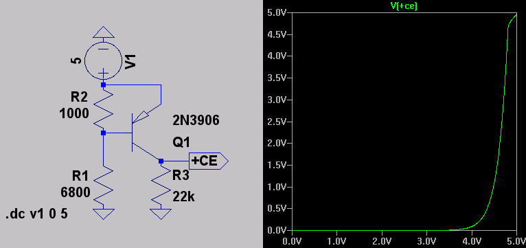
Alternatively, use this battery protection circuit, which I most recently saw on the Racermate bicycle PCB:
+5FromCartridgeEdge—1kish—PNPBase—5.6k—Gnd
edit:had these resistors backwards+5FromCartridgeEdge—PNPEmitter
PNPCollector—SRAM+CE—22k—Gnd
Image and curve from LTSpice.
Attachment:
 +ce.png [ 5.32 KiB | Viewed 2355 times ]
You can fiddle with the exact ratio of 5.6k to 1k resistors to trade off the best point of "shuts down permission to write to the RAM before any dirty writes from the CPU" and "doesn't randomly disable itself in response to instability on the +5V line". The simulation shows a corner at 6.8k->4.8V, 6.2k->4.4V, 5.6k->4.0V, 5.1k->3.7V, but real-world behavior probably won't align.
Note that the battery voltage is no-where in this circuit.
For the PNP transistor use almost anything: a 2N3906, 2N4403, BC557, &c.
edit: braino'd, listed an NPN instead of a PNP part #
That is a handy little schematic, thanks for sharing. One potential issue I that could be taken into account if trying to make it more universal. Clones don't operate at 5v, they're usually around 3.5v from what I've heard. I can only speak for my portable that runs ~3.4v IIRC. Probably a safe universal point to shoot for around 3.0-3.1v assuming the SRAM's datasheet supports. My napkin shows that's probably somewhere around 4.4k on R1. You're right though, it should be verified with the real deal and probably a small population of transistors. I'm planning to do this testing, once I get around to it I'll post my results in a separate thread.

