Hi!! I'm just trying to do a Legend of Zelda repro from a portuguese translated ROM by Hexagon I got from NesNinja site.
I used this board from "Gol de Craque", a Jaleco's Goal pirated version sold by Gradiente here in Brazil:
Front of the board:
https://drive.google.com/open?id=0B0OtM ... 0M5OE92LWcBack of the board:
https://drive.google.com/open?id=0B0OtM ... DU4cG1mblEI have done some rewiring on the board, following this schematics:
http://www43.tok2.com/home/cmpslv/Famic/Fcmp1.pngFor the ROM I used a P28f001, PRG RAM is a KMS6264A-12 and CHR RAM is a KM6264BL-10.
So far so good the game only boots if I add R1, a 10k resistor, as show in the schematics, but when I press start it just locks out.
If I leave it alone, it locks on the treasures screen.
I just can't imagine what can be wrong.
Anyone has any ideas of what can be happening?
Are the schematics I followed correct?
I've not put the battery on the board yet, but I think this could not be doing all this trouble.
Thanks in advance!
I'm not very familiar with what you are doing but depending on the size of the translation couldn't you just split the rom into 2 files and toss on two 27c801 and swap bin them and toss on a troy aikmen cart? Or is it too big a file for that?
The original game is 1Mibit, as is the
translation.
It's not SNES, one doesn't need 8Mibit 'PROMs.
The size is fine, it's just a 1mbit image. The memory you suggested AFAIK is a 8mbit.
A lot bigger than needed.
I'll try to use both RAMs with 2x the same ICs...
I don't see much logic in this but...
I'm just running out of ideas!
Maybe the cloned MMC1 has a glitched SRAM control logic...
Or there's some address lines incorrect?
I just had not touched the address and data lines...
Only the ROM's A16 and the control lines of the RAMs, should I mod it someway?
It's remotely plausible that the clone MMC1 emits WRAM/CE rather than WRAM+CE.
But I really don't know, it seems at least as likely that the chip-on-board is some non-MMC1 thing and that the original was mapper hacked for the original Gol de Craque port.
Yeah sorry I assumed this was snes. I should have read it a little better.
Can you use a normal ntsc donor? If you can nes open golf and golf power should be good donors. You would just rewire the prg as follows.
SNROM (mapper 1):
Bend up pins 1, 2, 24, 30 and 31 (or cut tracks 2, 24 and 30)
Solder pin 2 to hole 24 (A16)
Solder pin 24 to GND (OE)
Solder pin 30 to hole 1 (A17)
edit: that if for m27c eproms. Not sure about the eprom you use.
Unfortunately I am not familiar with the boards and chips you are using so I will not be of much help.
lidnariq, is there some way to confirm this?
AFAIK this MMC1 clone has both CE and /CE.
I don't know if it's functional.
Before doing this repro, I tried Chip n' Dale on this board.
I even had finished the game.
It may be just a subset of MMC1 though...
icemanxp300: Yeah! I could be using official NES carts, it even seems easier to mod.
But they are too expansive here, around 100 bucks each!
That's why I'm stuck with the cheap pirates, or it would be like declaring war on my wife! :-b
SLROM: MMC1 with CHR ROM
SKROM: MMC1 with CHR ROM and WRAM
SKROM with battery: MMC1 with CHR ROM and battery-backed WRAM
SGROM: MMC1 with CHR RAM
SNROM: MMC1 with CHR RAM and WRAM
SNROM with battery: MMC1 with CHR RAM and battery-backed WRAM
Both Chip 'n Dale games are SLROM. For The Legend of Zelda, you want SNROM with battery. For Zelda II: The Adventure of Link, you want SKROM with battery.
A MySQL configuration limit is preventing this post from appearing as intended. I will report it in phpBB issues.
Maybe try making a reproduction of an SKROM board?
Alternatively, could you use the pinouts on the wiki with a continuity meter
-
http://wiki.nesdev.com/w/index.php/MMC1_pinout-
http://wiki.nesdev.com/w/index.php/Mask_ROM_pinout-
http://wiki.nesdev.com/w/index.php/6264_static_RAMto see if the supposed chip-on-board MMC1 matches up?
SNROM "should" have both /CE (pin 11, actually CHR A16) and +CE (pin 6) outputs.
lidnariq wrote:
Maybe try making a reproduction of an SKROM board?
Will that work? Zelda uses onboard chr ram where as skrom has chr rom.
It'll work if you skip The Legend of Zelda and instead make Zelda II: The Adventure of Link.
Right, I just meant "test with another game"
What I have done to the board up to now (according to my to-do list):
PRG ROM:
Cut the trace to the old A16 on the 28 pin chip (22), bridged the trace to the 32 pin's chip pin 2.
Bridged the 32 pin IC pín 24 to pin 22.
Made 4 holes on the board, so I don't need to bend the IC pins.
CHR RAM:
Cut the pin 22 trace and bridged to /RD.
Bridged pin 20 to PA13.
Cut pin 27 trace (was going to MMC1 pin 9) and bridged to PPU /WE.
Disconnected pin 26 from MMC1 pin 8 and bridged to VCC.
Bridged pin 1 and 28.
PRG RAM:
Cut the trace on pin 22 and bridged to GND.
Cut the trace on pin 26 from MMC1 pin 22 and bridged to MMC1 pin 6.
Cut the trace on pin 27 from MMC1 pin 1 and bridged to MMC1 pin 17.
Cut the trace on pin 20 and bridged to MMC1 pin 11.
Bridged pin 1 and 28.
Cut the VCC trace and added a diode to it.
As far as I remember, I have not done anything else besides adding R1 and R3.
The traces I have cutted that were going to the PRG ROM where later rebridged to the ROM, leaving some more traces that goes to PRG RAM alone.
I'll try another game, it may be the translation that has some bugs...
Should change the PRG RAM (or WRAM) to the CHR RAM's same IC model be a good idea too?
Weird thing happened:
I changed the PRG RAM IC, so, both RAMs are the same part, speed...
At first it was the same, than I removed R1 and R2.
The game stopped locking on presentation, has some graphical glitches, but works.
Then, at the name entry there are 3 names wich I can't select.
I erased them all and tried to create a new one, but as soon as I finish the names appear again with weird chatacters and I can't start the game.
Is this game timing critical?
Why such difference with a slight faster RAM?
Very weird!!
After my vacations, I'll try to resume this project.
I'll try Metroid in this board this evening.
Just in case someone is interested in the results I got with Zelda, I'm posting some small videos on YouTube:
Intro:
https://youtu.be/qv0MgqCEbggName entry:
https://youtu.be/BuJ_kjjr-pwGameplay:
https://youtu.be/WJLmb4W9BtoI would be glad if someone could give me something to at least start debugging it.
Thanks in advance!!
Tried with Metroid.
Have similar bugs:
https://youtu.be/WvDrO7akS1sI'm out of ideas...
Where should I start searching? CHR RAM??
I tried to decode PRG RAM address, ended with this circuit, using a 74ls08.
Attachment:
 NES PRG RAM Decoder.png [ 1.4 KiB | Viewed 3654 times ]
It's working better, but in some rooms the platforms appear fine at first and then disappear or get mixed up.
Ocasionally some platforms or parts of the background change colors too.
Is this circuit implementation correct? I just used what I had at hand...
This seems to confirm my suspicions that it's kind of incomplete (or buggy) MMC1 clone.
I also tried to disable PRG ROM when writting PRG RAM using this circuit,(just added an 74ls04 to the mix) but ended with an unbootable cart:
Attachment:
 PRG RAM Proteção.png [ 1.43 KiB | Viewed 3654 times ]
I'll try to do some videos showing what's up later.
Hope someone can give some advice this time...
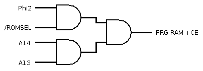
Fisher wrote:
Code:
M2 --+---_
| )---+
/ROMSEL -+---¯ +--+---_
| )--- PRG +CE
A14 --+---_ +--+---¯
| )---+
A13 --+---¯
[...]
Is this circuit implementation correct?
Looks right?
Note that /ROMSEL arrives later than M2, by enough to potentially be a problem.
It ought to be ok, but maybe as stands writes to the MMC1 register at $E000 could accidentally write to RAM as well.
You could try rearranging as
PRG RAM +CE = AND(AND(AND(M2,CPU A14),CPU A13),/ROMSEL) so that the propagation delay of M2 through the first two AND gates might match, and see if that fixes anything.
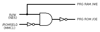
Quote:
Code:
CPU R/W ------+---_
| )---|>O--- PRG ROM /OE
MMC1 PRG ROM /CE --|>O-+---¯
I'm not clear why that's not working? But it's worth pointing out that the PRG ROM should already be disabled (i.e. the MMC1 should already be generating
MMC1 PRG ROM /CE = OR(NES /ROMSEL,NOT(CPU R/W)) )
Thanks for the attention

I have rearranged as you said and noticed no differences.
Should I add more logic to try to slow M2 down?
Maybe add a capacitor?
Fisher wrote:
(i.e. the MMC1 should already be generating MMC1 PRG ROM /CE = OR(NES /ROMSEL,NOT(CPU R/W)) )
I have tried it because I'm afraid that the RAM protection may not be implemented properly.
Maybe the LS04 I got is bad... I just got these parts from very old peripheral boards.
I think it may be some register data beig write to RAM, and not some bus conflict or RAM corruption. But I may be wrong...
Fisher wrote:
Should I add more logic to try to slow M2 down? Maybe add a capacitor?
I don't know

You're already using a 74LS part, which effectively has pullup resistors (transistors, really) on all its inputs.
You could try something like
Code:
M2 -|<|-+- 74LSxx input
|
gnd -C--+
which should delay M2 rising edges but not M2 falling edges
Anyway, Metroid writes to the PRG bank register via $E000, so if there were corruption of PRG RAM it'd be the byte at $6000. But Metroid is also a FDS port, so it writes to $E000 fairly rarely; if you're seeing tile corruption regularly and not just once, it's probably not that. More likely some other PRG RAM issue.
Tried the diode and capacitor, no difference.
Tried even a crazy RAM protection circuit made with an LS02:
Attachment:
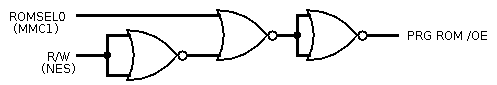 PRG RAM Proteção NOR.png [ 1.44 KiB | Viewed 3606 times ]
No deal too.

Let me try to explain exactly where the bug first appears:
I start and go left to get the morph ball, then, go all the way to the right.
The bug starts when I enter the room that I can go up.
At first, the platforms appear fine, when the transitional animation ends some appears a little down, others disappear and are seem just as a solid wall.
I can jump up on the invisible platforms. If I go up, the next screen seems just fine.
About 3 or 4 screens up some parts change from blue to orange.
This is as far as I go in the game, it may or may not have more bugs.
I hope I can do a little video tomorrow, it may show the bugs better.
Would this be CHR RAM related?
The only thing on CHR RAM I see connected on MMC1 is A12. Should I connect it straight to PPU A12?
Again, many thanks for helping. I'm learning a lot while having fun!!
... That sounds like mirroring control is broken?
The mirroring circuit inside the misterious black bubble?
Can I somehow build a substitute externally like the PRG RAM decoder?
What about CHR RAM? Is the connection to MMC1 CHRA12 correct?
Fisher wrote:
The mirroring circuit inside the misterious black bubble?
Yeah,
nesdevwiki:MMC#Control.
Quote:
Can I somehow build a substitute externally like the PRG RAM decoder?
Probably not
You could try burning a copy of tepples's
Holy Diver, Batman! test, and see what it says...
Quote:
What about CHR RAM? Is the connection to MMC1 CHRA12 correct?
Yes.
As I have understood, would be necessary to redo almost the entire mapper!!
I really will like to do this, but in the future. My knowledge is still very tiny.

I should have already made the ROM socketed. I was too confident when I modded it.

Or, maybe just give up and try a game that don't use the mapper's PRG RAM.
I was thinking in do a translated Megaman 2...
I'll try the Holy Driver tomorrow. I'll post here the results.
Again, many thanks!!
These are by far the best logical circuit classes I have get!!
Here's the video, some seconds before the first bug:
https://youtu.be/cotiQwsVMRA?t=1m32sA little before the second bug:
https://youtu.be/cotiQwsVMRA?t=2m55sThe video from the begining, it's boring see me playing Metroid:
https://youtu.be/cotiQwsVMRAHope this make easier to get some clues.
Thanks!
Yeah, that
definitely looks like the mirroring control is broken.
Do traces go between PPU A10, PPU A11, and CIRAM A10 to the black chip-on-board?
(
http://wiki.nesdev.com/w/index.php/MMC1_pinout ,
http://wiki.nesdev.com/w/index.php/Cartridge_connector )
Took a look at them.
They're connected according to the schematics I'm following, the same way they're shown on MMC1's pinout.
In fact, I have not touched these pins on my mod.
Looks like it has some internal register bug.
I had not removed the Flash ROM yet to try the holy driver.
Maybe I don't need to... just disconnect /CE and /OE from one chip and connect to another, making sure all the other pins match.
I think this can save me some time.
Holy driver Batman!
Looks like it's trying to comunicate!

Someone could please tell me what's he's saying?
Attachment:
Perharps there's some bad soldering somewhere!
Or maybe he just says: "give up you pirate" ?

The beeps spell out MIR. From the manual:
MIR
The nametable mirroring for this mapper doesn't match any of the supported mappers. Check PA13-PA10, /PA13, CIRAM A10, and CIRAM enable, and don't try running the 78.3 test on an emulator that does not support NES 2.0 format.
How expensive are random electronic components to you? I might be able to figure out something to implement the mirroring control using programmable logic (GAL20V8, 22V10, or maybe random 74xx parts), but whether that's worthwhile depends on what you have easy and affordable access to.
It depends of the parts.
Most stuff I have made are from parts I got from old peripherals or even junk.
Most parts are expensive here, since where I live is essentially a rural area.
The PAL chips need to be programmed, right? How hard is to do it?
I ask because for writting the flash ROMs I use an old PC motherboard.
Could this be used to write the PAL chips?
Maybe the best way would be with random 74xx logic.
If you help me, I'll be very happy!
I just took a look at the docs and can't even imagine how that stuff could be implemented!
Thanks in advance!
Fisher wrote:
The PAL chips need to be programmed, right? How hard is to do it?
It's not too hard, but you would probably need to build special hardware for it, e.g.
http://www.etc.tuiasi.ro/cin/Downloads/ ... atics.htmlQuote:
I ask because for writting the flash ROMs I use an old PC motherboard.
Could this be used to write the PAL chips?
Probably not; most flash ROMs only require a single voltage to program, but GALs always required multiple.
Quote:
Maybe the best way would be with random 74xx logic.
Uh, well, try this, I guess:
Attachment:
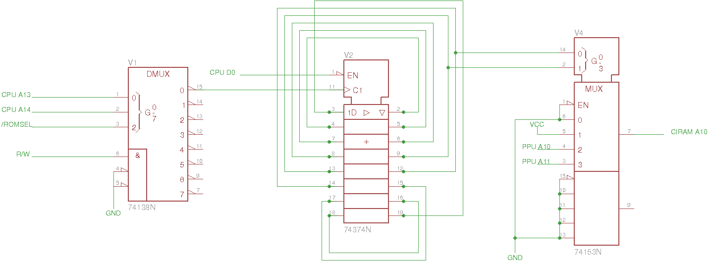
 mmc1-mirroring-control.png [ 2.19 KiB | Viewed 4193 times ]
Chip hunting season!!
As soon as I have some results I'll post here, as usual.
Many thanks for now!!
@Tepples:
Sorry. I've read the manual, but I just could not diferentiate traces from dots.
Looks like I need to train my ears at least to know who is who.
Anyways, I would like thank you, for this awesome program!!
As far as availability goes, there's a lot of available substitutions.
You can replace the 4002/74'4002 with a 74'138, 74'139, 74'23, or 74'25.
You can replace the the 74'164 with a 74'96, 74'198, 74'199, 74'299, &c
You can replace the 74'153 with a 74'253, 74'151, 74'153, &c.
I don't know whether mixing technologies from radically different eras (e.g. 74F with 74ACT) will work.
Well, I just can't get the 74'164 or similar.
Seems to not be much used on old PC motherboards.
I thought in trying to make something similar witn an 74'374 or maybe 2x 74'175, but the complexity of the circuit would be greater.
I'll try to order from Aliexpress... let's see if I can get the things before 3 months...
Anyway, looks like I've found another MMC3 clone.
I'll open another thread to discuss this.
Thanks for now. I'll try to build this as soon as I get all components.
I think we could probably get away with using an ordinary D-register (e.g. three 74'74, a 74'176, a 74'374, &c) as long as we have at least five bits of storage.
I'm worried about putting too many ICs on this.
First, because I'm doing a "spider" kind of assembly, second because I'm not sure of how many ICs can be powered safely on a NES cartridge?
I already have the ROM, 2SRAMs, the MMC1's clone, the decoding and protection circuit.
It's 6 ICs!!
If I add 6 more: 4x 74'74, a 74'138 and a 74'153 I'll have a very nice rat's nest and a cartridge that may consume too much power.
I've ried an 74'374 without success, it may be deffective... I just plugged the outputs on the inputs, plugging the last output on the first input. Is this idea correct?
Can somehing like this be made with an 74'373? I think Ican get one of these from an old NES that should be working...
Fisher wrote:
I'm not sure of how many ICs can be powered safely on a NES cartridge?
Depends on the specific technology of the 74xxx parts you're using. 74HC or 74AC you should be able to use a whole bunch. Plain no-letter variants, not so many.
Note that GALs are already much more thirsty than discrete logic, and some boards use
multiple GALs or
many many 74xx ICs, so I think this particular issue is unlikely to come up.
The standard front-loading US NES has a 1A 5V power supply, and uses 350mA of that for the CPU/PPU/&c. Obviously whatever you're using could vary...
Quote:
I've tried an 74'374 without success, it may be deffective... I just plugged the outputs on the inputs, plugging the last output on the first input. Is this idea correct?
Uh, maybe? Plugging 2D into 1Q, 3D into 2Q, &c, to make a shift register? That should work.
Quote:
Can somehing like this be made with an 74'373? I think Ican get one of these from an old NES that should be working...
No; the '373 is a transparent latch; when its +LATCH signal is high the value will just shoot right through all eight bits. This really needs registers with their clock input.
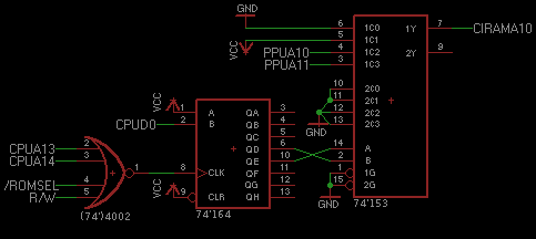
WOW!! That's quite a lot of random logic!!

I finally could draw the schematics of what I intend to do.
I'm trying Eagle, if you know a better/easier software that's Linux frienly please let me know.
Could this possibly work?
Attachment:
 mmc mirror.png [ 12.45 KiB | Viewed 3979 times ]
Looks like a little messed up.
I'm not sure who would be the A output, so I'm throwing a little guess...
I really like Lidnariq's design, it's a lot cleaner!!
Any chance I could get some free sample ICs from any manufacturer?
'374 should always be enabled.
CPU D0 should go to '374 1D.
You don't care about faked shift register after the two bits that go into the multiplexer. Since it's a register, you could even safely leave 6D..8D floating (but you should probably tie them to ground or +5V)
Otherwise looks right.
---
I keep on trying to like KiCAD, but I keep on finding it unusable. GEDA is ... better, but I still like Eagle more. Xfig and Xcircuit are ancient passable solution for schematics, but don't do layout at all. LTSpice (via wine) won't do layout, but does let you simulate things.
You're extremely unlikely to get free samples of any legacy part (like 74xx). You might be able to scavenge a GAL for free, though... but you'll have to find/borrow a programmer.
Back on this old topic again!!
Made the corrections as you told.
I'm having trouble drawing the PCB, it don't show the Vcc connection on the ICs.
What am I missing?
Attachment:
File comment: New schematics.
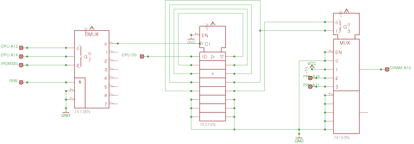 edited mmc1 mirror.png [ 12.63 KiB | Viewed 3811 times ]
Don't tie the '374 outputs to ground: leave them floating.
This looks like Eagle? If so, the 74xx ICs should have an implicit connection to "Vcc" and "Gnd" nets, and their power pins should already be connected to each other.
Sorry for the long delay, but this project is driving me nuts!!
I've built the circuit over 10 times and I always find to have one or two defective parts!!
Is there a way to know if a game uses this kind of mirroring switching before trying it on the real hardware?
I've tried Megaman 2 and some graphics appear glitched on the intro
I think this may be the same cause.
The idea of buying a cheap JRPG to do this mod is starting to appear good...
Anyway, thanks for the support, you're great!!
You can assume that anything using SGROM uses mirroring switching, as it's the only significant difference in overall capability compared to UNROM or BN/AOROM.
Yes I did. But unfortunatelly I end up discovering this bugged MMC1
I think there may be some games that don't use this feature.
I have a Chip'n Dale (1) working fine on a board very similar to this (with MMC1 implemented as an epoxy blob). I'm not sure if the games aren't hacked, but this board had Goal 2, the other was Stealth ATF, and if I remember well, I've seem Ninja Gaiden (1), Double Dragon (1) and Predator, all sold and manufactured by the same trademark: Gradiente/Falcom Soft.
I don't know if would be possible to figure it out with a debugger, or taking a look on the game's PRG data.
Looks like it's a matter of put sockets on this board and see what will work fine or not.
Well... As I have read in aother post,
quitters don't learn!!Looks like the '138 wiring is wrong here...
According to this
truth table, I would have 7 other conditions that would drive any of the outputs high.
I think the clock needs the transition from low to high.
I can't see how I could do this with an '138 without a inverter.
Can this be done?
The '374 latches its contents on a rising edge.
The '138 generates a low pulse on one /Y0 through /Y7 for the duration of all the six inputs matching. So, yes, it generates a falling edge when /ROMSEL falls, and a rising edge when /ROMSEL rises, and yes, that means it's a tiny bit delayed relative to the CPU's data bus ... BUT that shouldn't be a problem. The CPU's data bus should remain floating until after the value from the data bus is safely latched inside the '374.
So... again I'll start over...
I thought in give up of this board, but no! I'm learning a lot while trying to fix this
I think I should make a PCB for this thing, it would make troubleshoot easier.
The "spider" just confuses me more each time I need to check something.
I always need a multmeter to confirm what is soldered where.
Just a really big rat's nest
Try adding resistors and LEDs to the '374s outputs so you can see if it's actually working?
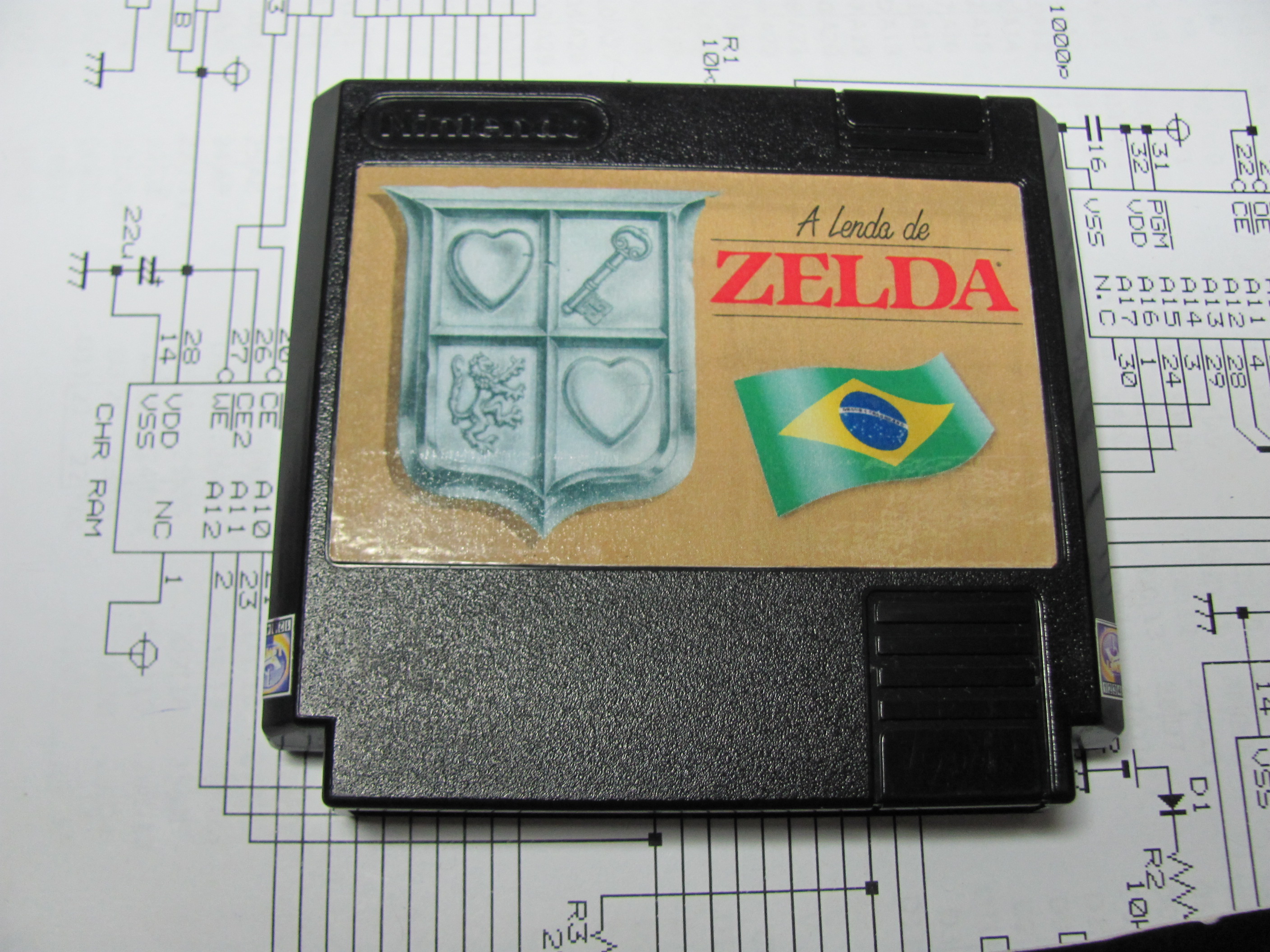
Finally!!
I could get a 100% working solution for my Zelda repro!!
Attachment:
File comment: Zelda BR - Frente
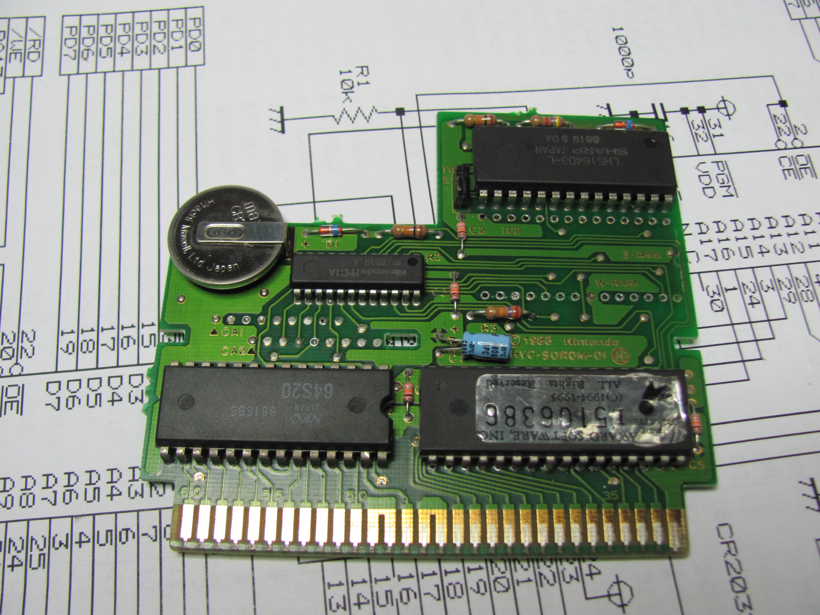 IMG_2075.JPG [ 1.38 MiB | Viewed 2490 times ]
Attachment:
File comment: Zelda BR - Solda
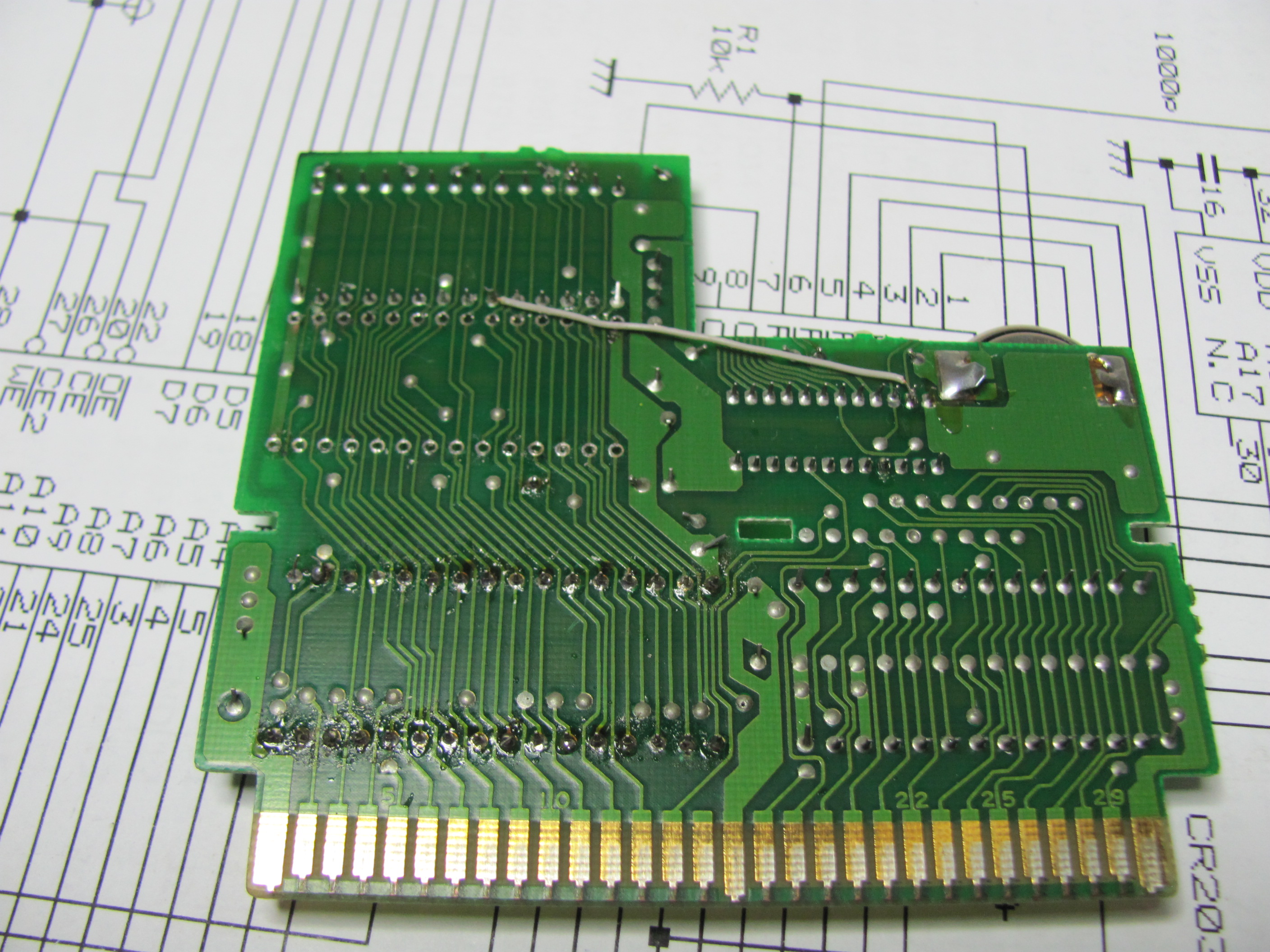 IMG_2078.JPG [ 1.39 MiB | Viewed 2490 times ]
Attachment:
File comment: Zelda BR - Montado
 IMG_2079.JPG [ 1.42 MiB | Viewed 2490 times ]
Unfortunatelly I had to kill a Famicom original, that's something I'm not very proud of
It was Nobunaga No Yabou, and, as far as I could know, this was a kind of boring action RPG, just like Royal Blood, that I'm planning to do a Castlevania 3 repro on it. Anyway I'm saving the original maskroms, just in case I need to undo these mods in the future... who knows what the furure reserves!!
I took in account many opinions posted here, mostly the Bregalad's ones, wich I agree most of the time.
Although the other board has a bugged (or should I say cut-down) version of the MMC1, I now know some games that work fine with this setup. This include Stealth ATF, Chip 'n Dale, Goal! and even the buggy Bionic Commando ROM I've flashed.
Surprisingly, the Bionic Commando takes a lot more time to crash in that board.
Any suggestion about some trick I could use to debug it?
The game don't seems to crash on emulators, even Nestopia, wich I think is one of the most accurate emulators around.
Many thanks guys!!
I've learned a lot of things while trying to make these repros.
In special, from you Lidnariq and Tepples you guys really rocks!!
Both you and many others around have a huge knowledge and are nice enough to share!!
Again, many thanks guys!!