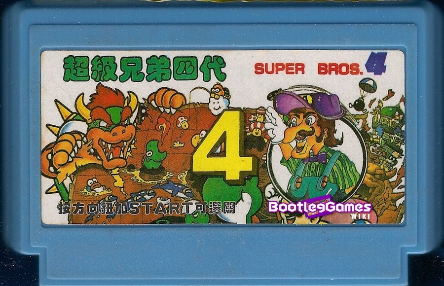
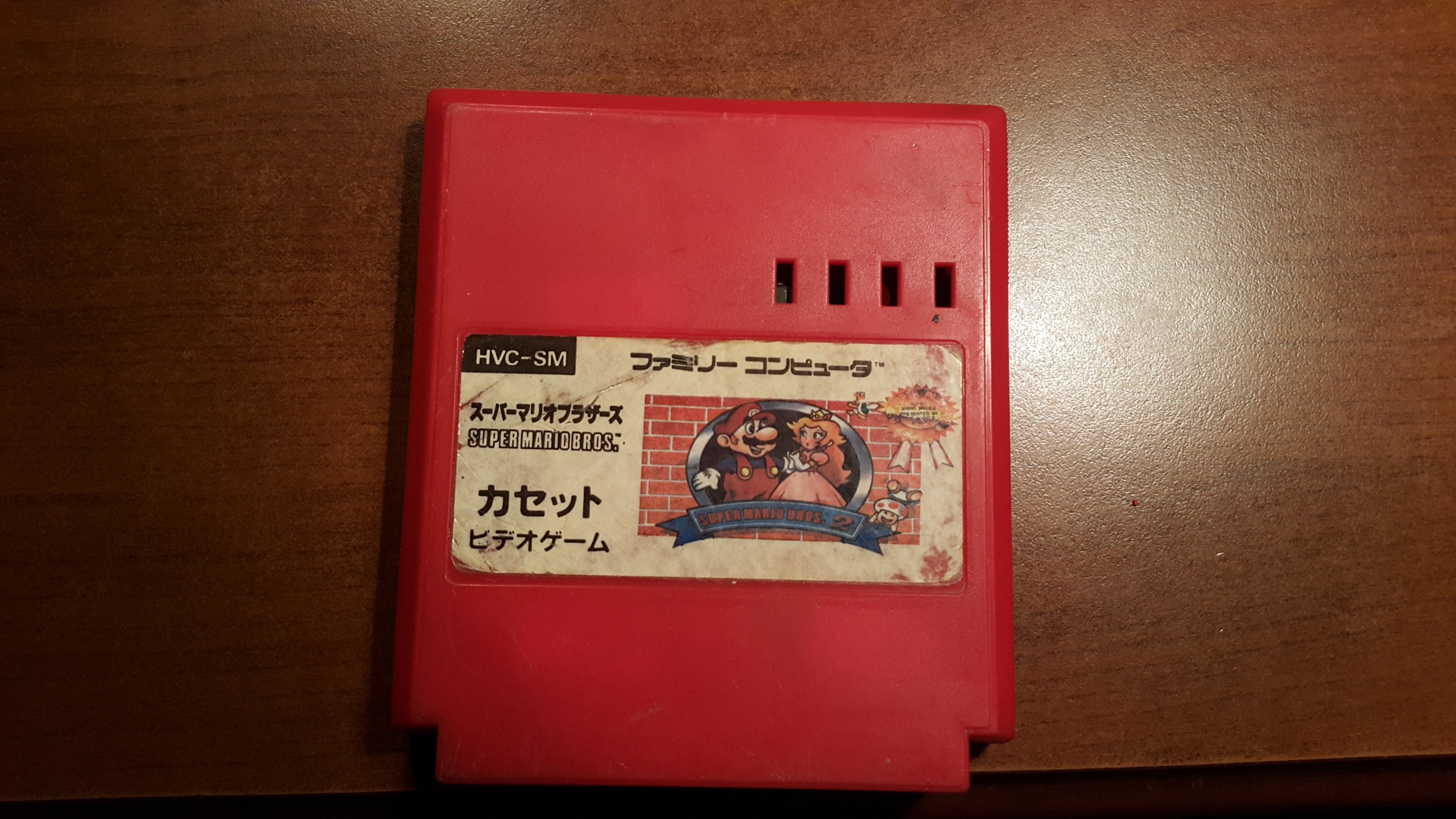
Super Mario Bros 2 JAPANESE (a'ka Lost Levels) is quite interesting game. It was officially released only on Famicom Disk System floppy disk and those cartridge versions that exists are pirate ports from FDS. There exists many ports which are using different hardware solutions and thus - are emulated under different mapper numbers, like
http://wiki.nesdev.com/w/index.php/INES_Mapper_040
http://wiki.nesdev.com/w/index.php/INES_Mapper_050
and probably many others.
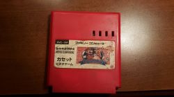
There are some examples of actual cartridges:


Quite interesting fact is that even the total size of memories used on such cartridges differ. Probably it consists of FDS Bios (modified) and dumped PRG/CHR from floppy.
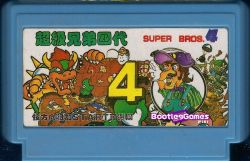
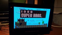
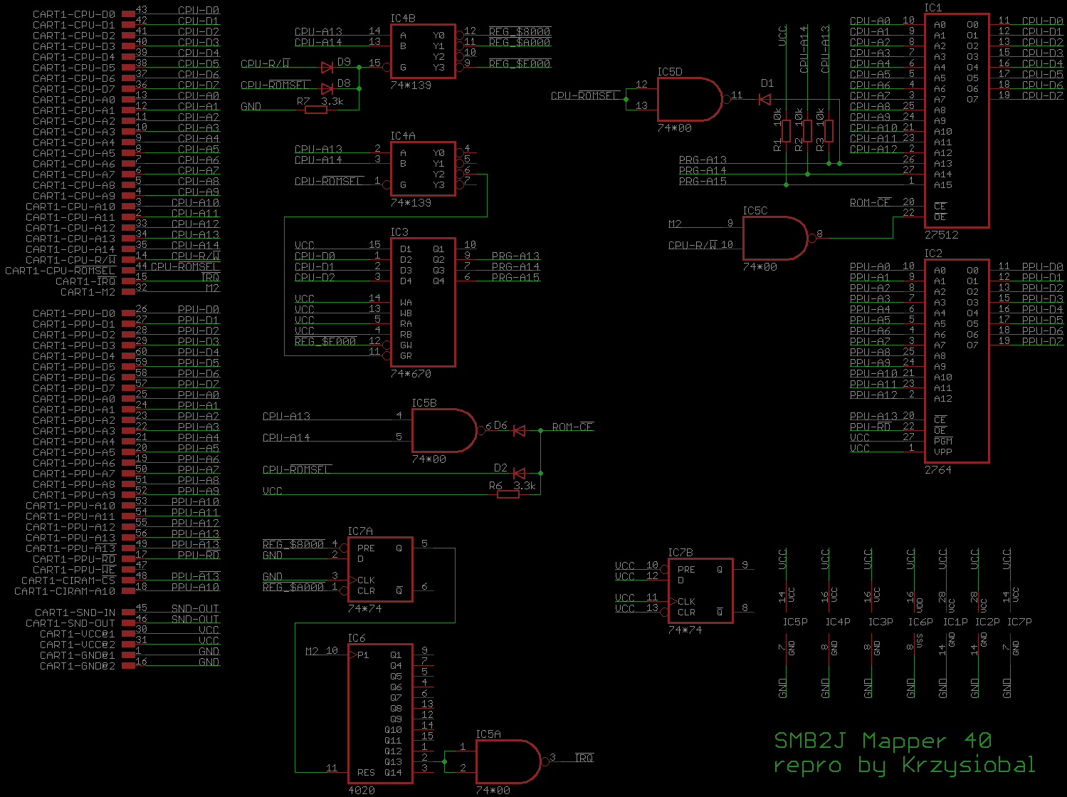
I was asked to make reproduction of Super Mario Bros. 4 (FDS Conversion)(Unl)[!] (which is hack of SMB2J that runs on mapper 40). The mapper is quite simple and as a good exercise I did not want to make it on FPGA, but use as little discrete discrete chips as possible.
Mapper overview:
Ok, so here is my brief thoughts how I would do that with a list of chips that I would probably need:
* 4020 + 1/2 7474 -> IRQ counter + IRQ ack & en/dis
* 1/2 74139 -> decoding $8000/$a000/$c000/$e000 for writes
* 74670 -> register to store PRG bank (I needed one with three state outputs)
* and probably one/two gates as glue logic
But how to make this fancy fixed-banks? Well, let's look at it in the binary:
Now it reveals why I wanted three state outputs register - if we are not in $c000, we can use pullup resistor to force value of PRG lines to:
PRG A15 <- 1
PRG A14 <- CPU A14
PRG A13 <- CPU A13 when /ROMSEL = 0 else 0
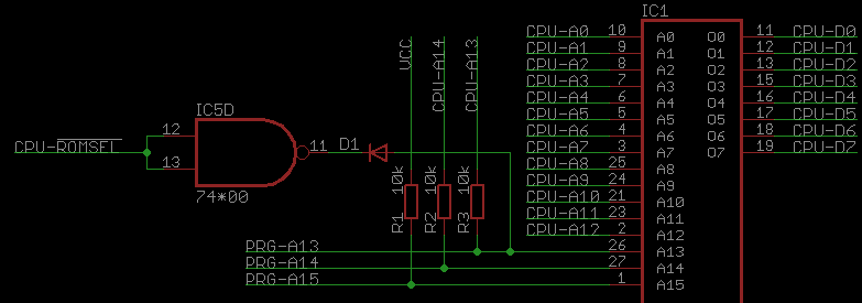
What about the `else` part of PRG A13? Diode can be used as a second branch of `if`:
There are some minor things to do:
* Activate PRG-ROM at $6000-$FFFF + prevent bus conflict
* Activte register outputs only at $c000-$dfff
All of this I did using only 2/4 of 7400 + some dide logic
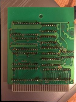
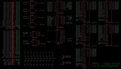
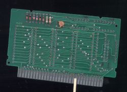
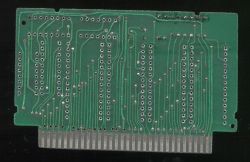
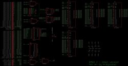
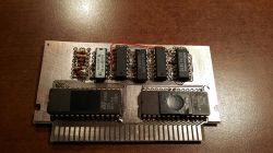
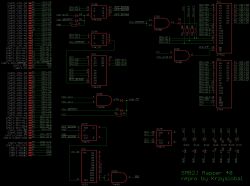
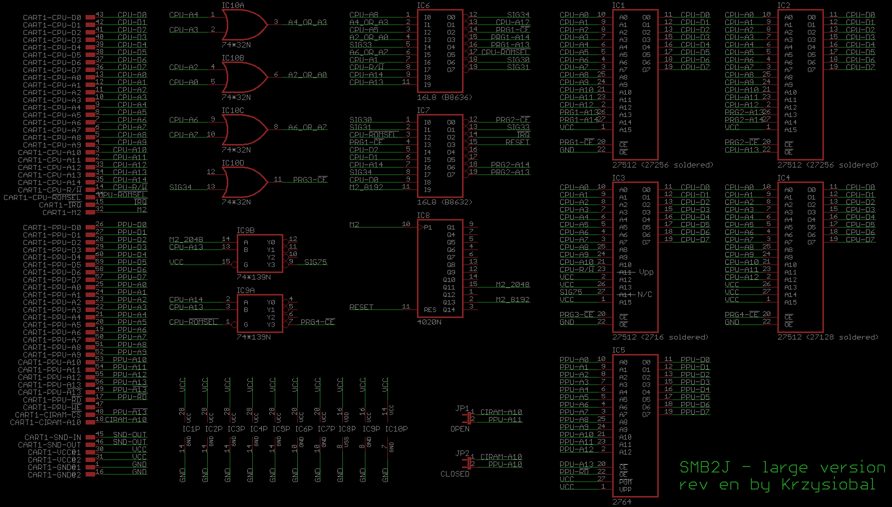
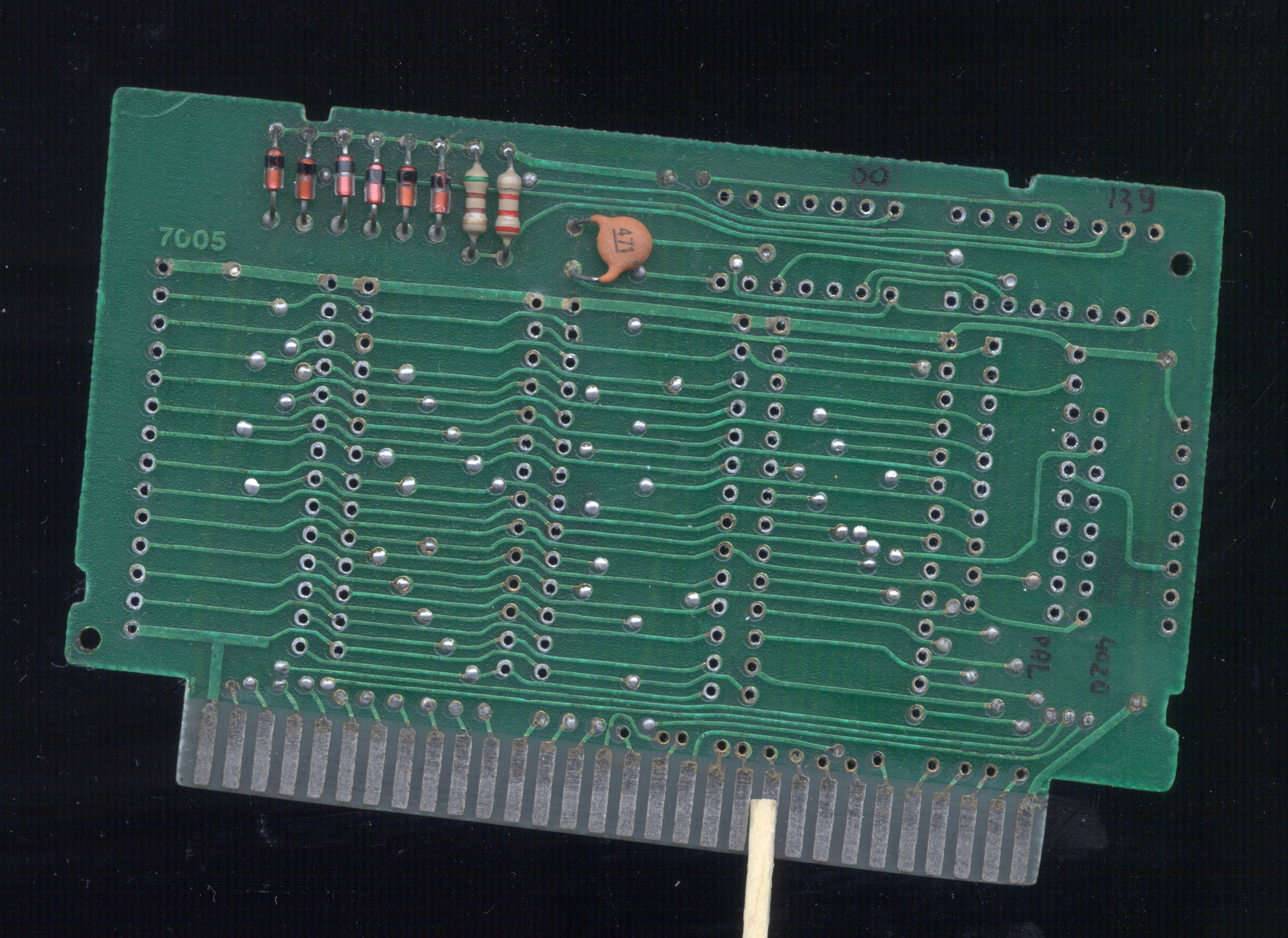
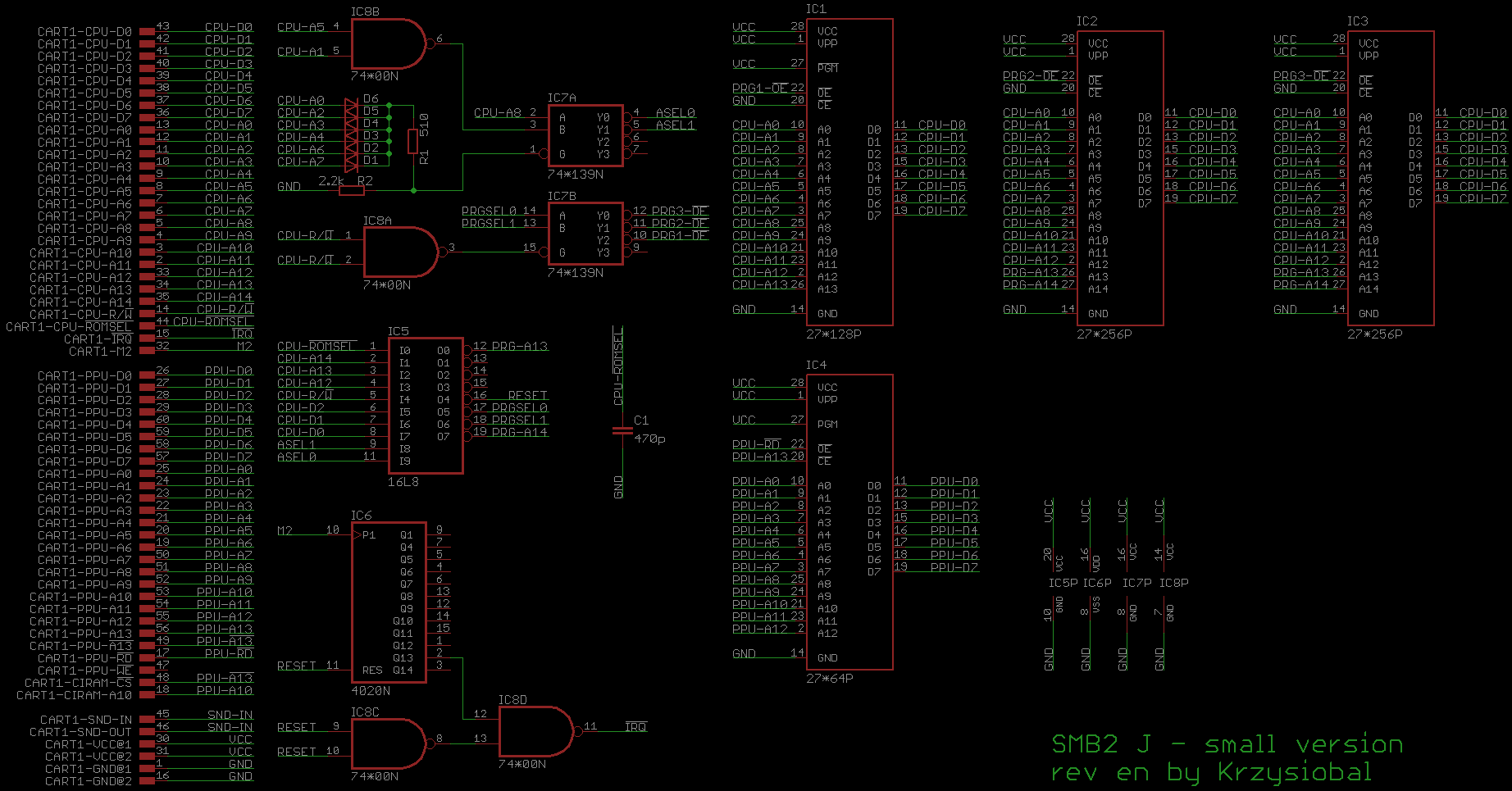
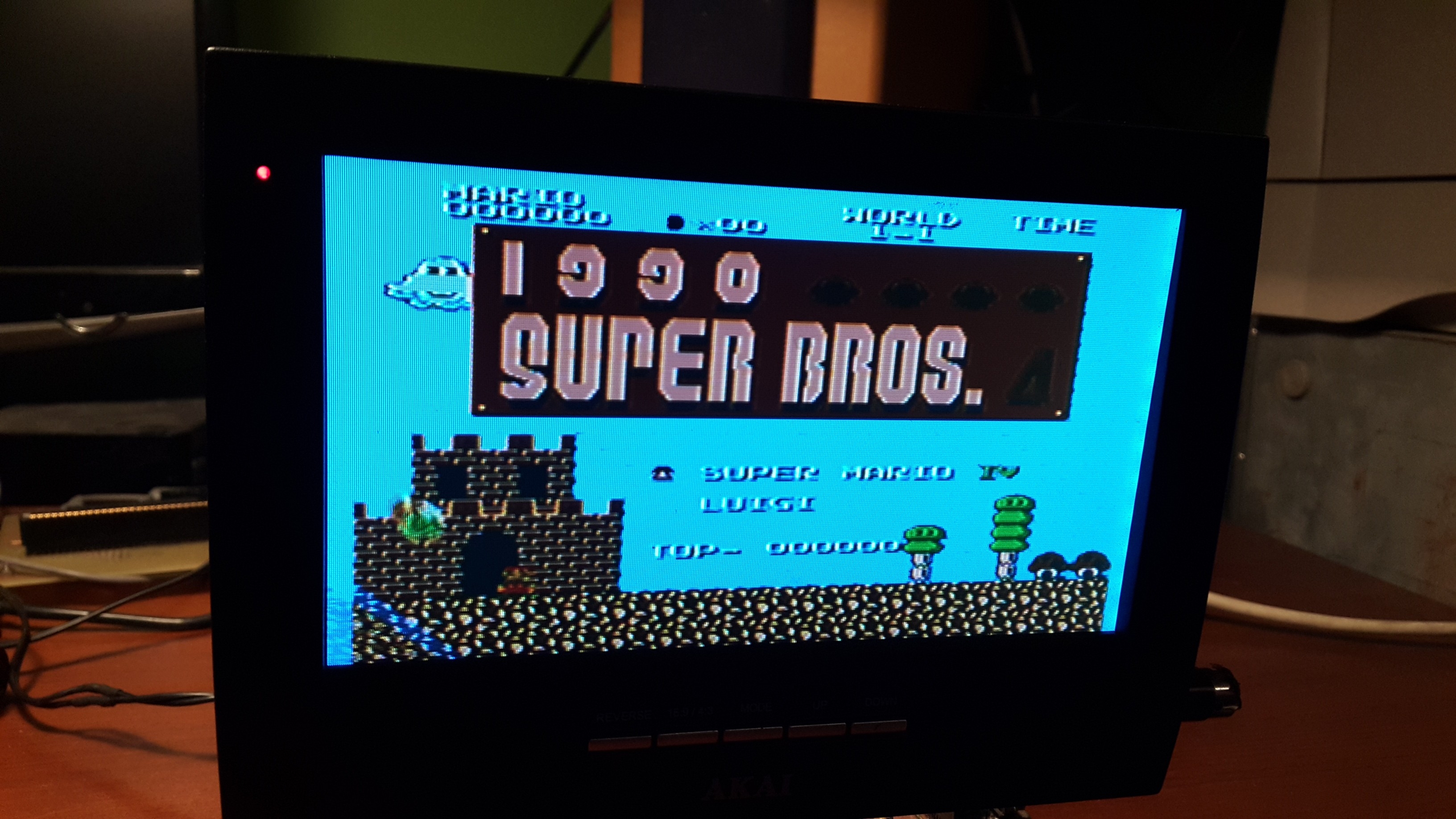
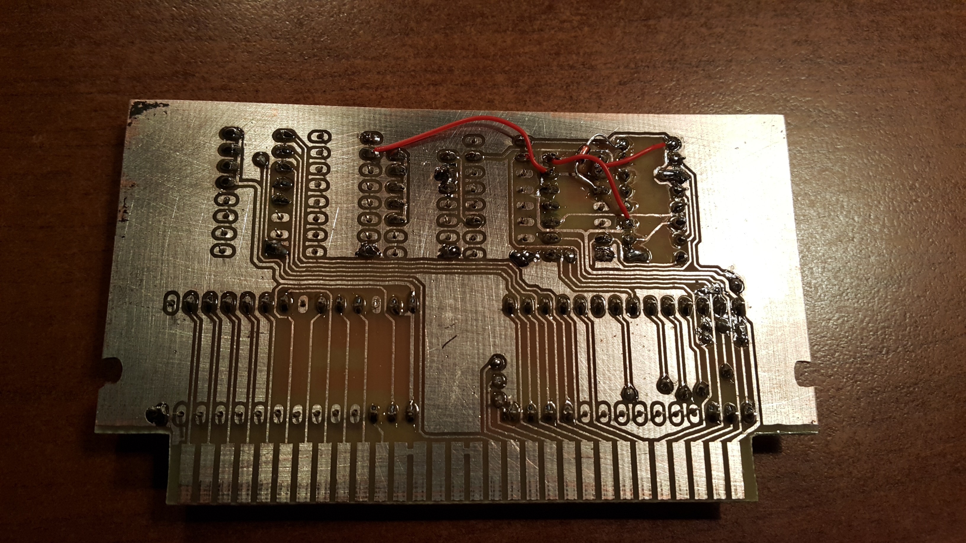
Here is final schematics + photos of final version of cartridge:

I still have 1/2 of 7474 not used, which can be used as.. poor man's NOT gate ;D
---
Cartridge has not started since first run, because:
* I forgot to solder some of the ICs pins at TOP layer (when making double side PCB, i prefer to trace it that way so all chips are soldered only at bottom side. Other connections are made by wires acting as vias), but this time I wanted to make as little vias as possible and use chip leg's as vias
* I forgot to add inverted between 4020's output and /IRQ
* I connected 4020's Q12, instead of Q13,
* Those diode AND/NOT are not the best use. Firstly, I used 1k resistors, but voltage drop on diode for 0 logic level was too much (~0.8V). After switching to 3.3k it is ~0.7V (which should be sufficient),
* The 2764 EPROM used as CHR-ROM caused troubles during programming (I had to program it many times to change all bytes into correct values). But it still gives inconsistent reads, I need to replace it.
http://wiki.nesdev.com/w/index.php/INES_Mapper_040
http://wiki.nesdev.com/w/index.php/INES_Mapper_050
and probably many others.
There are some examples of actual cartridges:
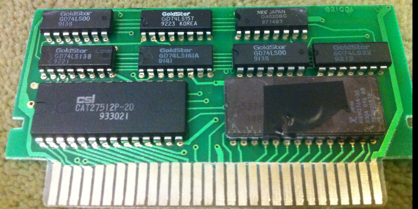
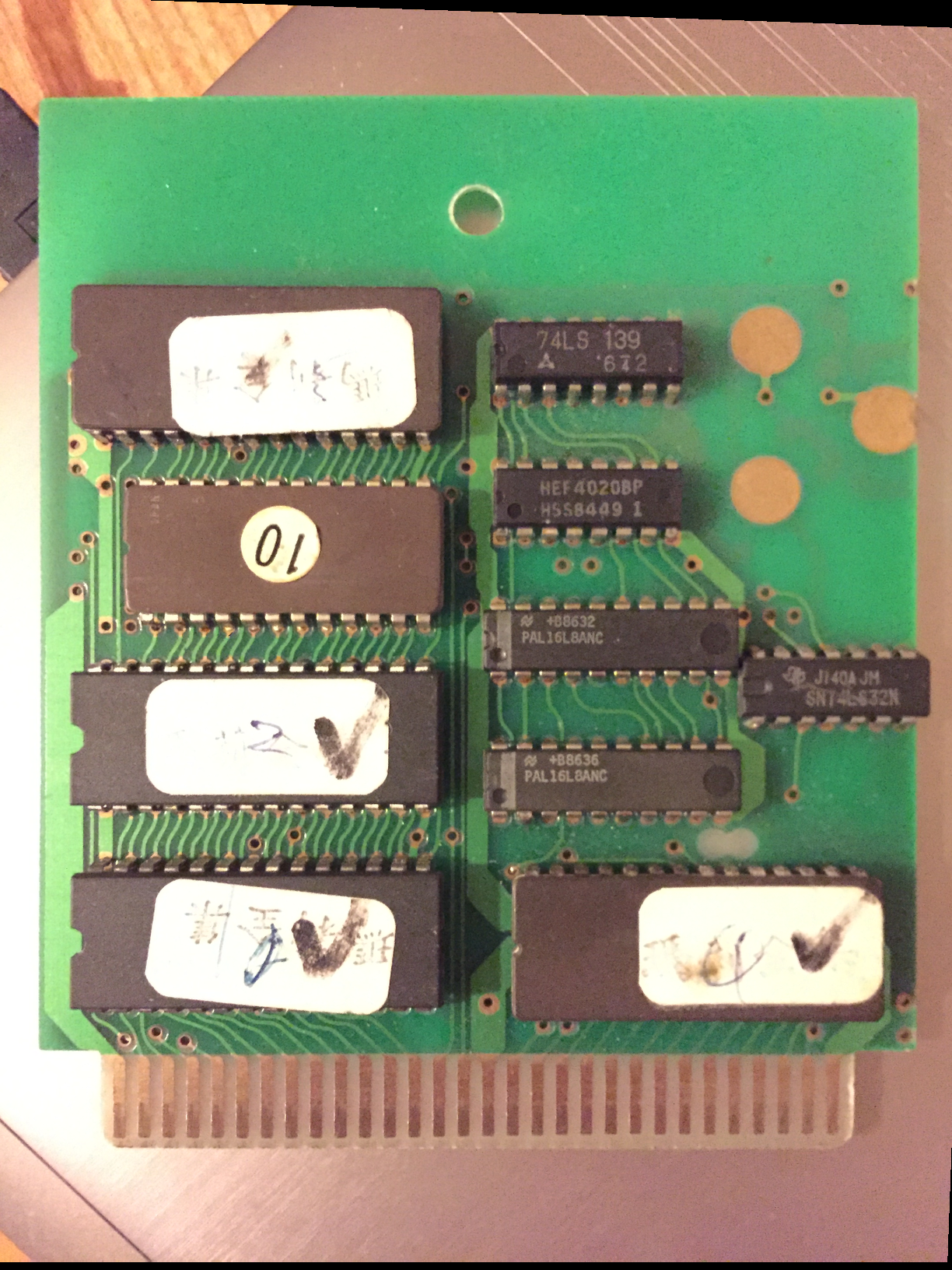
Quite interesting fact is that even the total size of memories used on such cartridges differ. Probably it consists of FDS Bios (modified) and dumped PRG/CHR from floppy.
I was asked to make reproduction of Super Mario Bros. 4 (FDS Conversion)(Unl)[!] (which is hack of SMB2J that runs on mapper 40). The mapper is quite simple and as a good exercise I did not want to make it on FPGA, but use as little discrete discrete chips as possible.
Mapper overview:
Code:
Range,Mask: $8000-FFFF, $E000
$8000: Disable and acknowledge IRQ
$A000: Enable IRQ
$E000: 8 KiB bank mapped at $C000
PRG Setup:
---------------------------
$6000 $8000 $A000 $C000 $E000
+-------+-------+-------+-------+-------+
| { 6 } | { 4 } | { 5 } | $E000 | { 7 } |
+-------+-------+-------+-------+-------+
$8000: Disable and acknowledge IRQ
$A000: Enable IRQ
$E000: 8 KiB bank mapped at $C000
PRG Setup:
---------------------------
$6000 $8000 $A000 $C000 $E000
+-------+-------+-------+-------+-------+
| { 6 } | { 4 } | { 5 } | $E000 | { 7 } |
+-------+-------+-------+-------+-------+
Ok, so here is my brief thoughts how I would do that with a list of chips that I would probably need:
* 4020 + 1/2 7474 -> IRQ counter + IRQ ack & en/dis
* 1/2 74139 -> decoding $8000/$a000/$c000/$e000 for writes
* 74670 -> register to store PRG bank (I needed one with three state outputs)
* and probably one/two gates as glue logic
But how to make this fancy fixed-banks? Well, let's look at it in the binary:
Code:
BANK /ROMSEL CPU CPU | PRG PRG PRG
A14 A13 | A15 A14 A13
-----------------------+------------
$6000 1 1 1 | 1 1 0
$8000 0 0 0 | 1 0 0
$a000 0 0 1 | 1 0 1
$c000 0 1 0 | * * *
$e000 0 1 1 | 1 1 1
A14 A13 | A15 A14 A13
-----------------------+------------
$6000 1 1 1 | 1 1 0
$8000 0 0 0 | 1 0 0
$a000 0 0 1 | 1 0 1
$c000 0 1 0 | * * *
$e000 0 1 1 | 1 1 1
Now it reveals why I wanted three state outputs register - if we are not in $c000, we can use pullup resistor to force value of PRG lines to:
PRG A15 <- 1
PRG A14 <- CPU A14
PRG A13 <- CPU A13 when /ROMSEL = 0 else 0
What about the `else` part of PRG A13? Diode can be used as a second branch of `if`:
There are some minor things to do:
* Activate PRG-ROM at $6000-$FFFF + prevent bus conflict
* Activte register outputs only at $c000-$dfff
All of this I did using only 2/4 of 7400 + some dide logic
Here is final schematics + photos of final version of cartridge:

I still have 1/2 of 7474 not used, which can be used as.. poor man's NOT gate ;D
---
Cartridge has not started since first run, because:
* I forgot to solder some of the ICs pins at TOP layer (when making double side PCB, i prefer to trace it that way so all chips are soldered only at bottom side. Other connections are made by wires acting as vias), but this time I wanted to make as little vias as possible and use chip leg's as vias
* I forgot to add inverted between 4020's output and /IRQ
* I connected 4020's Q12, instead of Q13,
* Those diode AND/NOT are not the best use. Firstly, I used 1k resistors, but voltage drop on diode for 0 logic level was too much (~0.8V). After switching to 3.3k it is ~0.7V (which should be sufficient),
* The 2764 EPROM used as CHR-ROM caused troubles during programming (I had to program it many times to change all bytes into correct values). But it still gives inconsistent reads, I need to replace it.