This is just an idea I had.
Each PPU fetch takes 2 cycles (the actual fetch occuring on the second cycle), and each CPU cycle takes 3 PPU cycles.
This would mean that, for each CPU cycle, there is always at least 1 PPU cycle where the PPU is not fetching, in which time, the fetch can go to the CPU instead.
During the phase where the PPU is not fetching, the RAM's address and data lines can be routed to the CPU instead. If the CPU wants to write, it can all pass through. If the CPU wants to read however, the byte fetched from the ram would need to go to a latch, which would feed the CPU's data lines. This is because the byte would need to be held on the CPU's data lines until the CPU is finished making the fetch, and the PPU making a fetch would disrupt this.
This would hypothetically allow one ram chip to feed both the PPU and the CPU. The obvious advantage is that the memory is accessible by both busses simultaneously. That means you can prepare some graphics memory in the CPU's address space and then swap it into the PPU, freeing you up from vblank bandwidth and allowing you to prepare offscreen buffers.
The requirement would be RAM that has a quick enough response time to be usable at the PPU's clock rate, since the address would be changing every PPU cycle, alternating between the CPU's and the PPU's busses.
Are there any reasons why this wouldn't work? If not, I was going to draft it into
my mapper design. 32kb of memory usable as pattern tables, nametables, extended attributes, and general purpose wram, together with vblank-agnostic video updates would be an incredibly powerful feature.
I remember playing around with that idea a while back, the trouble for me was that I didn't know how to tell which cycle the PPU is on. There's the /ALE signal, but that doesn't come out to the cartridge. I guess a delay thing could be done, based on the PPU /RD or /WR signal, but I'm not sure of the best way to get that, or is there another way you have in mind?
This is a great idea! I, as a programmer, would love to have a big chunk of VRAM that could also be used as WRAM in any way I saw fit. I can't contribute to the hardware design at all though, since that's not my area of expertise, so sorry! =)
Isn't this what dual port RAM is for? Why do you need to get funky with the PPU timing?
I think this is an attempt to provide a dual-port-like front-end to "normal" 6264/62256 SRAM, giving the CPU access while PPU /RD is high (inactive). It sort of reminds me of the multiplexing of memory between video and CPU in the Commodore 64 and Apple II. The only dual-port RAM that I've seen used in NES Game Paks is the ExRAM in the MMC5. What other dual-port RAM is affordable?
Yeah, it's an attempt to multiplex "normal" ram which, as Tepples said, is more easily available than dual-port ram. Also, on other systems where actual dual-port ram is used for both the CPU and the graphics, accessing the graphics memory during rendering causes "snow" artifacts to appear on screen, so my method shouldn't have those glitches since there's only one access at a time.
This information on the wiki, specifically "During this cycle, the value is read from or written to the lower eight address pins", I'm lead to believe that there's a possibility that during the first cycle, neither the /rd nor /wr pins are asserted, since the PPU is outputting a garbage address. Performing a write at that time would be destructive, and performing a read would result in bus conflicts as the PPU is trying to latch the lower 8 bits of the address, from pins that are multiplexed as both address and data lines. I have no idea if this is true though.
In any case, you'll have to isolate the PPU address bus from the memory while the CPU is accessing the memory and vice versa. This would probably require a buffer IC as big as the MMC5.
tepples wrote:
In any case, you'll have to isolate the PPU address bus from the memory while the CPU is accessing the memory and vice versa. This would probably require a buffer IC as big as the MMC5.
A data selector wouldn't work? Both busses go into the selector, and one pin on the selector determines which bus gets connected to the RAM. That way, both busses connect to the RAM. When either PPU /RD or PPU /WR are asserted, the PPU's bus is selected, with the CPU selected otherwise.
Granted, the mapper's banking pins would have to be routed to the selector as well, so it'd be a lot of pins, but it's not a hugely complicated circuit.
What you mean by "data selector" is what I meant by "buffer IC". The address lines alone would need 39 pins (13 from CPU, 13 from PPU, 13 out to RAM), plus a bunch more for select lines. It'd have to latch the data bus too in order to satisfy the CPU's setup and hold timing if it services a read from the CPU close to a read from the PPU. So with the majority of the cart bus as well as all RAM signals, you're looking at a minimum close to 80 pins.
Multiplexing the I/O is the easy part. To expand on what I posted earlier, it seems like the real trick to this is in how the control signals for the memory will be generated. PPU /RD and /WR is easy, it's faster and will have to take priority, but the /RD, /WR, and /CE pulses for the CPU accesses will have to come from somewhere. I can see how to do it with an FPGA or a CPLD with a counter in hardware, you'd have a fast clock input and could arbitrate the memory access and generate the control signals based on periods of that clock. I've done a little planning on a mapper that would work like this. Before I started using programmable logic, I used to try to figure out how to make this work with 74HC parts but was never able to, without bringing in some kind of expensive hardware to help.
The NES CPU memory can be really slow, a Game Genie I modified is running my code on a 450ns EPROM. Seems to work OK at that speed.
On a related note, it's worth considering that the CPU writing to memory is slower than writing to the $2007 port. Now you need addressing modes, you lose the auto-increment, etc. But OTOH, writes to VRAM are generally being pre-buffered in RAM by the CPU anyways.
Pre-buffering works if you don't need random access. But for anything resembling LZ77 compression, you need random access if you're going to be using back-references longer than 256 bytes. You also need random access if you're planning to store parts of the game state in unused parts of VRAM.
tepples wrote:
But for anything resembling LZ77 compression, you need random access if you're going to be using back-references longer than 256 bytes.
Why are you mentioning this arbitrary amount of memory like it was the absolute maximum anyone would dedicate to this purpose?
I don't see why someone with less game state to keep track of couldn't decide to use 512 or more bytes for their LZ buffer. On the other end, another programmer might have so little free RAM that he can't even spare 64 bytes.
And there's also the actual decoding process to consider... if speed isn't a concern, one can very well read and write through $2006/$2007, setting the address for every byte if necessary (I did this once, I think), but using a small buffer to copy strings isn't out of the question.
Here's the logic in English, I'm not in the right mind right now to try to figure out the physical connections for these though:
Select the PPU's address bus only when the PPU is reading or writing (PPU_/RD && PPU_/WR), or when the CPU is accessing outside of $6000-$7FFF. Select the CPU's address bus otherwise. The currently selected address bus determines whose turn it is.
Enable the CPU's outbound buffer only when the CPU is writing during its turn. Tri-state it otherwise.
Enable the CPU's latch only when the CPU is reading from WRAM, regardless of turn. Tri-state it otherwise.
Clock the CPU's latch only when the CPU is reading during its turn.
Enable the PPU's outbound buffer only when the PPU is writing. Tri-state it otherwise.
There's no situation in which you'd need to block inbound data coming to the PPU, but in case you wanted to be safe:
Enable the PPU's inbound buffer only when the PPU is reading. Tri-state it otherwise.
Edit: Sorry, I forgot to mention: In order to control chip communications on bidirectional busses, you'd need two buffers per chip; one for incoming data, and one for outgoing data. Having just one buffer would mean that data can go one way but not the other way. So for example, the CPU would have a buffer where RAM_D0-D7 is connected to the inputs and CPU_D0-D7 is connected to the outputs, and also a buffer with CPU_D0-D7 at its inputs and RAM_D0-D7 at its outputs. Therefore, one buffer regulates the "outbound" data and the other buffer regulates the "inbound" data. (and in my case, the CPU's inbound buffer is actually a latch)
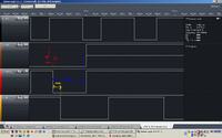
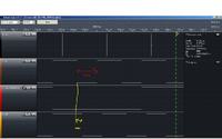
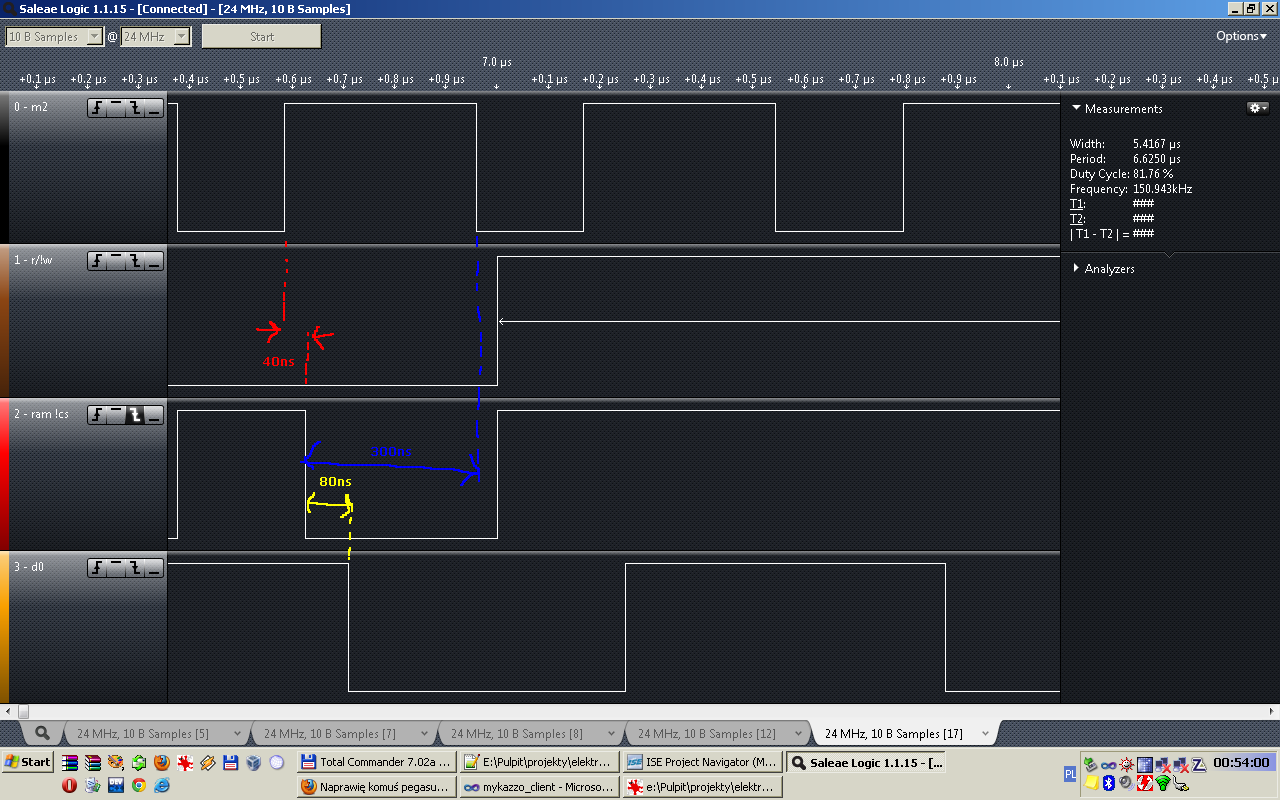
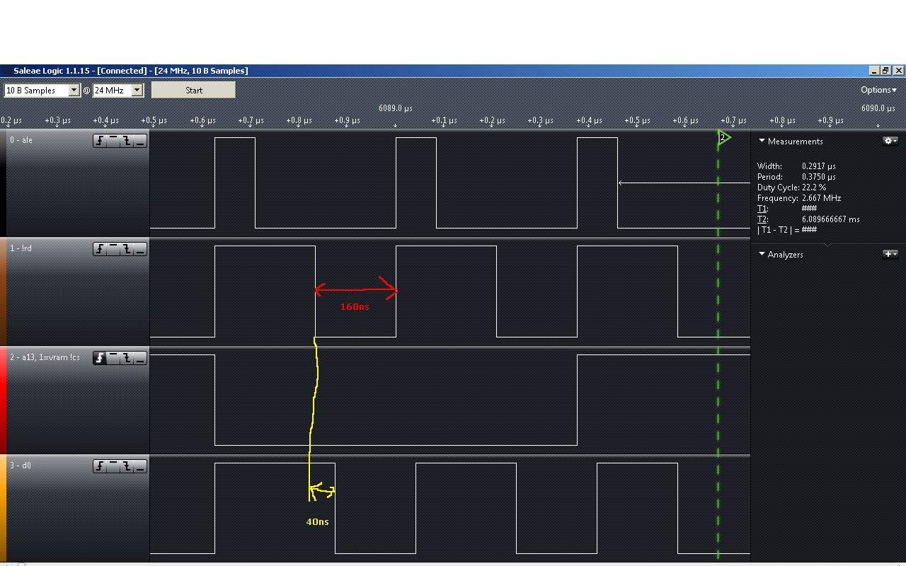
Question is, can the 2A03 correctly receive data at these two alternate duty cycles? The timing tolerances of the cartRAM can certainly be changed by selecting a different part, but the CPU, not so much.
The buffer chip could latch the 8-bit data read back from the memory, much like
registered memory, and ensure that it's stable on the CPU data bus by the time M2 is about to fall. Show me a logic analyzer trace of M2 and PPU /RD, and I'll try to clarify how it might work.
Nah, that makes sense now. Haven't been getting enough sleep, you know how finals are. Got the mapper between the buses (so that it has pins for RAMD0-7, PPUD0-7, CPUD0-7), and you latch the RAM value from RAMD to CPUD; thus on the 2/3 PPU cycles the data-read will be on CPUD0-7 between 1/3 and 2/3 of the M2 pulse, and on 1/3 cycles it'll be there between 2/3 and 3/3 of the M2 pulse.
That sound about right?
Yep, that was the idea.
Edit: I just noticed that my previous post was missing some information about what I meant by "inbound" and "outbound", sorry if that confused anybody.
I just checked visual 2C02, and indeed, both /wr and /rd are unasserted during one cycle of a fetch, and /rd is asserted during the other. When accessing the PPU bus via $2007 with rendering off, it appears that the memory accesses aren't aligned in any meaningful way, but there will always be periods of /wr and /rd both unasserted between accesses.
So that means you can indeed use (ppu_/rd && ppu_/wr) to determine whether the PPU is making a fetch or not, and there will always be at least one "rest" cycle between ppu fetches. That means, for each CPU cycle, there will always be at least one PPU cycle where the PPU isn't fetching, allowing the CPU to make a fetch to the same memory, provided the CPU's address and data signals don't reach the PPU and vice versa.
Shared memory between the CPU and PPU is indeed possible!
Edit: Just found out that this is called "cycle stealing". In this case, the CPU is cycle-stealing the PPU without interrupting the PPU.
tepples wrote:
What you mean by "data selector" is what I meant by "buffer IC". The address lines alone would need 43 pins (15 from CPU, 13 from PPU, 15 out to RAM), plus a bunch more for select lines. It'd have to latch the data bus too in order to satisfy the CPU's setup and hold timing if it services a read from the CPU close to a read from the PPU. So with the majority of the cart bus as well as all RAM signals, you're looking at a minimum close to 80 pins.
Of course, probably using a larger RAM than 15 address lines supports, if one uses it for everything. So, pretty much all cart edge (72) minus CIC (4 pins) PPU/A13 (1) and EXP pins (9, if you've got audio mapped), and duplicate ground (1). (/IRQ is probably left in for other mapper purposes, but is not needed for this application.) 57. Plus fifteen(+) for RAM-A0-15(+) is back to 72, and plus 8 for RAM-D0-7 is 80. Plus at least a pair of RAM/CE, RAM R/W, RAM/WR, RAM/RE. Looks like 82, plus more for bigger RAMs. And yeah, at least 2*(8D+15A)=46+1 latch/status bits, though I suppose optimization/routing means you only need 24 or 5 as the latch will only ever be going one way at a time...hmm...
The MMC5 had 100 pins, so I know it's not crazy to go up that far.
All of the the CPU and PPU address lines (including romsel) would need to go into the IC so the IC can output the correct 15-bit address to the RAM. The upper lines of the CPU and PPU address are also used in determining which bank registers to output. For PPU, this doesn't result in any extra pins because it goes towards the 15-bit ram address. For CPU, this results in 8 additional pins going to PRG (A13-A20).
The RAM also needs a pair of access lines, and the PRG needs an OE line.
So pretty much every pin of the Famicom cartridge connector would need to go to the mapper, plus 8 address lines output to the PRG, plus 3 control lines for the RAM and PRG, plus 15 address lines for the RAM.
Removing the multiplexed ram feature would cut down on the pins since most of the address lines from the CPU and PPU could then go straight to the ROMs, with only the upper address lines driven by the mapper.
So yes, you're right, this mapper would have a large amount of pins, but I think the functionality would be worth the investment.
Drag wrote:
So yes, you're right, this mapper would have a large amount of pins, but I think the functionality would be worth the investment.
Is it worth hundreds of thousands of dollars to make an ASIC? Answers to
this question on Electrical Engineering Stack Exchange states that each revision of a "normal" (standard-cell) ASIC can cost up to $500,000, plus the price of the industry-standard non-free software to verify your design. A gate-array ASIC can cost only $35,000 to master but that's not much cheaper than just using an FPGA.
For that much money, you could just make your game for the Super NES, where you have 128K of work RAM and 6K of bandwidth to VRAM per frame.
Doesn't need to be an ASIC. An FPGA-based board just needs to be able to boot faster than the CIC, or if that's not possible, to at least provide a small stable ROM in PRG space until the FPGA has initialized.
So how much would a suitable (over 80 pin) FPGA and flash to hold the bitstream cost per unit?
Assuming we just want to do the simplest possible "share 8KiB CHR-RAM with CPU as though it were also PRG-RAM", the cheapest FPGA with at least (13+8+2)×3=69 I/O is the iCE40LP1K-CM121 and the iCE40HX1K-VQ100. It needs 5V I/O translation and power supplies, and MIGHT need a four-layer board, so all in all it's probably about $6-7 of parts cost.
On the other hand, since you've already paid for the 3V translation, you can probably save a little money on the ROM and/or RAM.
Then again, a lot of FPGAs already have fast synchronous RAM inside of them, so you may be able to just skip the external RAM altogether.
There's no way I'd actually be creating a real ASIC from all of this, I'd only go as far as FPGA, or CPLD if the mapper complexity and cost allow it.
If the multiplexer for the RAM address were external, the mapper would no longer need CPU_A0-A12, and would no longer need to output RAM_A0-A9. Instead, the mapper can simply output a bus-select signal to the multiplexer. That'd be a 22-pin reduction. This is if and only if pin count were a problem, because an external 15-bit multiplexer would add 4 ICs to the board.
Drag wrote:
This is if and only if pin count were a problem, because an external 15-bit multiplexer would add 4 ICs to the board.
But you don't need to go all the way. One 74'157 exchanges twelve lines through the programmable logic for a single control line; each additional 74'157 saves another twelve lines without needing another control line.
You might be able to use analog multiplexers (e.g. 4053 or 4551) for the data bus, also. (Depends on what the on-state resistance is)
The cheapest CPLD on digikey right now is 1.8V logic, which requires "Real" translation rather than taking advantage of TTL voltage thresholds (i.e. unlike 3.3V logic), and it only has 54 I/O, requiring it to be matched with two external 74'157s.
To avoid any voltage translation, the cheapest 5V-tolerant I/O anything is either a Silego Greenpak, or Xilinx's XC9500XL series. The Greenpaks are noticeable smaller (in terms of I/O and total logic complexity) but cheaper. Either way, they're both small enough you'd have to outsource most or all of the multiplexing behavior.
I was very excited about this at first, but looking at the complexity of the solution, I have to say it's very disproportionate to the benefits. If you could pack this feature into an MMC5-like super mapper, then maybe this would be worth it, but by itself, I don't think so.
By itself? You mean 32kb multiplexed ram on NROM? Yes, that'd be pretty ridiculous. However, this isn't about putting this one feature on NROM, it's about fleshing this concept out so it can be used at all. There's plenty of proof that this is feasible, and even if I haven't figured out the most optimal way to fit it on my mapper design, that doesn't mean nobody else is allowed to figure out how to get it to work on theirs.
What you could do is have the mapper output Bus_Select and /Bus_Select, so that you can wire two seperate RAM chips, one for the PPU and one for the CPU, by wiring these lines to the RAMs' /CS (or whatever equivalent). The cycle-stealing logic will still operate, but this way, you have the option of having seperate PPU/CPU RAM, or having multiplexed RAM, with the multiplexed RAM setup requiring the external address multiplexer.
Hmm, we were having a similar discussion about taking those <50ns Async SRAMs and using them as 'effective' multiport memory by using a CPLD or FPGA, that would (probably) also double as the mapper chip. This hardware setup would also be useful for stuff like a debugger. A different firmware for the 'mapper' would give you something like JTAG support?
A year ago, someone simply replaced the NES's 2 KiB internal RAM with a dual-ported RAM –
http://www.batslyadams.com/2014/05/nes- ... rface.html – for similar effects.
The cost of a dual-port RAM is higher, but not tremendously so, than the FPGA we'd need to fake it.
What about making the timing a lot more coarse? Could either of these two be effective?
1. What if the CPU is only allowed to use it during vblank or rendering off, and the PPU us only allowed to use it during rendering? I mean, basically the same access windows as going through $2007, but without using $2007. Maybe the auto-increment on $2007 would make this a wash...
2. What if it was a double buffer of two RAM chips that you can swap during NMI, allowing CPU access throughout the frame? You'd have to switch all the address lines, but you wouldn't have to worry about "cycle stealing".
I'm not certain this is really a timing problem ... sure, because the NES provides /ROMSEL instead of A15 makes it kinda a pain, but if the interface was mapped to the same subset in both the bottom and top 32KiB it wouldn't matter. Because the PPU is 3x as fast as the CPU, there's always guaranteed to be at least one ALE cycle during which the CPU can write to the memory.
Making the timing less strict only helps with CPU reads, because the current constraint is M2 and the different CPU/PPU phases.
As near as I could tell, the problem with the other ideas was that Drag didn't like the amount of PCB footprint...
That said, the PowerPak has 3 KiB of (really really fast) internal synchronous RAM that could be dynamically attached to either bus, and it just needs a comparatively simple fusemap to use it...
I was fine with the footprint, but everyone else was telling me that it was too large and too expensive, hence the external multiplexer, but I don't know anymore. The bottom line is that this concept
will work, it's just a matter of implementation at this point, and implementation is historically the thing nobody ever agrees on.

You don't have to agree with anybody if you're going to do it yourself. ^_^
Well, as I said, the powerpak does have 3KiB of SSRAM internally, so if you have a powerpak and are willing to write some HDL you could play around with it.
Perhaps we should have somewhere to collaborate on/collect mapper theory and design?
I will try to do that on xilinx xc9572xl cpld. Here are the waveforms for read & write cycles from real famiclone's cpu (ua6527p) and ppu (ua6538):