So, I know CPLD are available, but it's complicated to use, requires the usagae of advanced software whose maitaining is in itself a problem, and there is no widely accepted chip that has guaranteed posterity (actually no electronic chip ever does, but heh, some more than others).
The PAL22V10 on the other hand is simple and extremely versatile. It also is 5V TTL compatible, however it comes with limitations, there can not be more than 10 flip-flops per chip. There cannot be more than 22 inputs and 10 outputs, and if a flip-flop is used in any output then every output must be a flip-flop, i.e. a whole chip is either combinational or synchronous as a whole. (*) Back when I wrote this topic, I knew squat about PALs, but now that I actually know them (at least better) I think it is possible to emulate the MMC1 perfectly with 4 PAL22V10 chips, and it does not require any other chips (exept maybe a SRAM backup specialized circuit).
The MMC1 needs 4 registers of 5-bits, so this takes up 2 chips (sequential). It also need output logic (combinational) and the 5-bit shift register (sequential). So a full MMC1 will take up 4 chips, if I am not mistaken. It might be possible to use other chips instead for parts of this, but since you have to buy PAL22V10s anyway, it's simpler to use them exclusively and not use any chip of the 74 series for instance.
In the case of a CHR-RAM board such as a SGROM or SNROM clone, the 2 middle MMC1 registers becomes useless if CHR-RAM bankswitching is not used (which is only the case in Romancia), and as such a chip can be removed, the MMC1 can be emulated with only 3 PAL 22V10 chips.
If it is somehow acceptable that writes to the shift register actually writes to the register directly, then the input shift register chip can be ruled out. This means a MMC1 in 3 chips for CHR-ROM, or 2 chips for CHR-RAM.
So it is probably possible to get a MMC1 with a relatively low number of relatively highly available chips, after all. That gus in the thread I linked to who says it needed "dozen" of PAL22V10 chips was definitely wrong.
EDIT: So there is it finally, the shema/diagram of what I mean. It takes one more chip than expected, so 5 PAL22V10s for a full MMC1! I am 90% sure this is technically feasible, however I might have messed up.
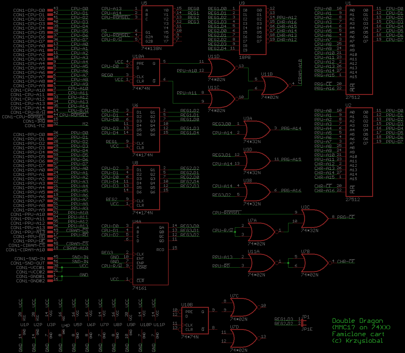
The function of the chips are as following:
A major issue is that the state at reset is not defined, therefore any bank can be mapped to the RESET/NMI/IRQ vector.
The PAL22V10 on the other hand is simple and extremely versatile. It also is 5V TTL compatible, however it comes with limitations, there can not be more than 10 flip-flops per chip. There cannot be more than 22 inputs and 10 outputs, and if a flip-flop is used in any output then every output must be a flip-flop, i.e. a whole chip is either combinational or synchronous as a whole. (*) Back when I wrote this topic, I knew squat about PALs, but now that I actually know them (at least better) I think it is possible to emulate the MMC1 perfectly with 4 PAL22V10 chips, and it does not require any other chips (exept maybe a SRAM backup specialized circuit).
The MMC1 needs 4 registers of 5-bits, so this takes up 2 chips (sequential). It also need output logic (combinational) and the 5-bit shift register (sequential). So a full MMC1 will take up 4 chips, if I am not mistaken. It might be possible to use other chips instead for parts of this, but since you have to buy PAL22V10s anyway, it's simpler to use them exclusively and not use any chip of the 74 series for instance.
In the case of a CHR-RAM board such as a SGROM or SNROM clone, the 2 middle MMC1 registers becomes useless if CHR-RAM bankswitching is not used (which is only the case in Romancia), and as such a chip can be removed, the MMC1 can be emulated with only 3 PAL 22V10 chips.
If it is somehow acceptable that writes to the shift register actually writes to the register directly, then the input shift register chip can be ruled out. This means a MMC1 in 3 chips for CHR-ROM, or 2 chips for CHR-RAM.
So it is probably possible to get a MMC1 with a relatively low number of relatively highly available chips, after all. That gus in the thread I linked to who says it needed "dozen" of PAL22V10 chips was definitely wrong.
EDIT: So there is it finally, the shema/diagram of what I mean. It takes one more chip than expected, so 5 PAL22V10s for a full MMC1! I am 90% sure this is technically feasible, however I might have messed up.
The function of the chips are as following:
- IC1 = Shift register. PAL is in sequential mode
- IC2 = Register 0 and 3. PAL is in sequential mode
- IC3 = Register 1 and 2 . PAL is in sequential mode (note, they are in this order because it's more practical for the schematic, but they could be made to be 0, 1, 2, 3 easily if required).
- IC4 = Output logic for control signals and PRG-ROM higher adresses. PAL is in combinational mode.
- IC5 = Output logic for higher CHR-ROM adresses (this is essentially a multiplexer that implement 4k bankswitching) PAL is in combinational mode.
A major issue is that the state at reset is not defined, therefore any bank can be mapped to the RESET/NMI/IRQ vector.
Code:
PPU A10 -----------------------------------------------------------------------------------------------+
PPU A11 ----------------------------------------------------------------------------------------------+|
PPU A12 ---------------------------------------------------------------------------------------------+||
+----------------------------------------------------+ |||
| IC1 PAL22V10 | IC2 PAL22V10 ||| IC4 PAL22V10
| .`````\/`````. | .`````\/`````. ||| .`````\/`````.
M2 ---+---|> CLK/IN1 | +-------|> CLK/IN1 | ||+----| IN1 |
(unused) -| IN2 IO1 |---> Parallel out D0 --------+-----|-------| IN2 IO1 |-->(reg3 D0) ---. |+-----| IN2 IO1 |---> CIRAM A10
/ROMSEL -| IN3 IO2 |---> Parallel out D1 --------|+----|-------| IN3 IO2 |-->(reg3 D1) ---.`-|------| IN2 IO2 |---> PRG /CE
CPU R/W -| IN4 IO3 |---> Parallel out D2 --------||+---|-------| IN4 IO3 |-->(reg3 D2) ---.`-|------| IN2 IO3 |---> WRAM CE
CPU D0 -| IN5 IO4 |---> Parallel out D3 --------|||+--|-------| IN5 IO4 |-->(reg3 D3) ---.`-|------| IN2 IO4 |---> PRG A14
CPU D7 -| IN6 IO5 |---> Parallel out D4 --------||||+-|-------| IN6 IO5 |-->(reg3 D4) ---.`-|------| IN2 IO5 |---> PRG A15
(unused) x| IN7 IO6 |---x Ctr D0 (internal only) ||||| | +--| IN7 IO6 |-->(reg0 D0) ---.`-|------| IN2 IO6 |---> PRG A16
(unused) x| IN8 IO7 |---x Ctr D1 (internal only) ||||| | +-|--| IN8 IO7 |-->(reg0 D1) ---.`-|------| IN2 IO7 |---> PRG A17
(unused) x| IN9 IO8 |---x Ctr D2 (internal only) ||||| | |+|--| IN9 IO8 |-->(reg0 D2) ---.`-|------| IN2 IO8 |<--- /ROMSEL
(unused) x| IN10 IO9 |---- Parallel load enable ---|||||-|--|||--| IN10 IO9 |-->(reg0 D3) ---.`-|------| IN2 IO9 |<--- CPU A13
(unused) x| IN11 IO10 |---x (unused) ||||| | ||| x| IN11 IO10 |-->(reg0 D4) --+ `-|------| IN2 IO10 |<--- CPU A14
(unused) x| IN12 | ||||| | ||| x| IN12 | |CPU|R/W --| IN2 |
`............` ||||| | ||| `............` | | `............`
||||| | ||| | |
||||| | ||| IC3 PAL22V10 | | IC5 PAL22V10
||||| | ||| .`````\/`````. | | .`````\/`````.
||||| +--|||--|> CLK/IN1 | | +------| IN1 |
+||||----|||--| IN2 IO1 |-->(reg1 D0) --|----------| IN2 IO1 |--> CHR A12
+|||----|||--| IN3 IO2 |-->(reg1 D1) --|----------| IN3 IO2 |--> CHR A13
+||----|||--| IN4 IO3 |-->(reg1 D2) --|----------| IN4 IO3 |--> CHR A14
+|----|||--| IN5 IO4 |-->(reg1 D3) --|----------| IN5 IO4 |--> CHR A15
+----|||--| IN6 IO5 |-->(reg1 D4) --|----------| IN6 IO5 |--> CHR A16
||+--| IN7 IO6 |-->(reg2 D0) --|----------| IN7 IO6 |--x (unused)
CPU A14 -----------------------------------------------------|+---| IN8 IO7 |-->(reg2 D1) --|----------| IN8 IO7 |--x (unused)
CPU A13 -----------------------------------------------------+----| IN9 IO8 |-->(reg2 D2) --|----------| IN9 IO8 |--x (unused)
(unused) x| IN10 IO9 |-->(reg2 D3) --|----------| IN10 IO9 |--x (unused)
(unused) x| IN11 IO10 |-->(reg2 D4) --|----------| IN11 IO10 |--x (unused)
(unused) x| IN12 | +----------| IN12 |
`............` `............`