Schematic for UM6561?

This is an archive of a topic from NESdev BBS, taken in mid-October 2019 before a server upgrade.
View original topic
Schematic for UM6561?
by on (#186048)
Well first of all HAPPY NEW YEAR :beer:

I want to make a mini Famicom clone by using UM6561 + two EPROM so that I can run simple NROM games on it.
I am testing the circuit on a breadboard :

Image


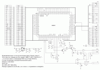
I found a Dendy schematic which is based on UM6561 but it seems it has some errors in it :
(capacitor signs are Russian : MK=uF / H=nF / n=pF)

Image


Fortunately I have a Famicom clone named FUMA-001 which uses the same chip :

Image

Image


By comparing them I found out that their circuit is very different so I have to compare them with another famous Famicom schematic :

Image


Also I want to omit RF and its related parts so that the whole thing become more compact.
Re: Schematic for UM6561?
by on (#186049)
Dendy :
Image

Fuma :
Image

Famicom :
Image

80sFREAK :
Image

Output :
Image

console5.com :
Image

Output :
Image
Audio
by on (#186050)
Dendy :
Image

Fuma :
Image

Sample Music - Rockman 5 - Blues no Wana! (J)
Re: Schematic for UM6561?
by on (#186051)
7805 official datasheet suggest to use 0.1uF and 0.33uF but in Dendy and Famicom they used 47uF and 470uF :

Dendy :
Image

Fuma (it seems caps are swapped wrongly?) :
Image

7805 Datasheet :
Image
Re: Schematic for UM6561?
by on (#186052)
Dendy (suggests to use 470nF (=0.47uF) Electrolytic capacitor) :
Image

Fuma (uses 100nF Ceramic capacitor) :
Image

Famicom (suggests to use 0.47uF Electrolytic capacitor) :
Image

so which one should I use?
Re: Schematic for UM6561?
by on (#186055)
Famicom :
Image

Dendy (both caps for crystal are 30pF) :
Image

Fuma (Caps are different 39pF and 12pF) :
Image
Re: Schematic for UM6561?
by on (#186056)
FARID wrote:
7805 official datasheet suggest to use 0.1uF and 0.33uF but in Dendy and Famicom they used 47uF and 470uF :
I've seen different specified capacitances there, depending on the nature of the input voltage and the technology of the capacitor.

Larger capacitances are needed when you have full- (or half-) wave rectified AC and the capacitor has to hold enough power to keep everything running for up to 10ms between mains.

On the low side, a better ESR will improve AV quality.

FARID wrote:
Dendy (suggests to use 470nF (=0.47uF) Electrolytic capacitor) :
Fuma (uses 100nF Ceramic capacitor) :
Famicom (suggests to use 0.47uF Electrolytic capacitor) :
so which one should I use?
On the 2A03 (I can't speak for the Dendy parts), the reset pin has a depletion NMOS pullup inside. When I measured mine, that pin emits somewhere between 20 and 50 µA continuously, only vaguely a function of the output and supply voltages.

The choice of capacitor only determines how long the CPU is held in reset after power up or after the user presses the reset button. A larger value will take longer.

The specific value doesn't seem to matter much, as long as the CPU comes out of reset consistently.
Re: Schematic for UM6561?
by on (#186112)
It works fine :

https://youtu.be/P-ByTSWdE84

Schematic Rev 2 :
- Better circuit for Video output
- Fixed some mistakes
Re: Schematic for UM6561?
by on (#186939)
I designed a PCB for my new project (United Famicom = Famicom + TxROM)
Which parts should be separated because of noise?
Re: Schematic for UM6561?
by on (#186946)
Most of the system is low-speed 5V digital, and thus pretty immune to any kind of crosstalk.

However, the analog signals—audio and video—are quite sensitive. Coax is probably overkill, but you wouldn't go wrong with the PCB equivalent (ground traces on both sides of the signal, and ground fill underneath)
Re: Schematic for UM6561?
by on (#187941)
So here is the United Famicom Rev 1.0 :
https://youtu.be/SadSu7zy3zw

The PCB costed about 50$
Re: Schematic for UM6561?
by on (#187942)
What's the point of making so long traces (GND polygon pour underneath helps from getting noise?)

How do u metalize holes?
Re: Schematic for UM6561?
by on (#187959)
Quote:
What's the point of making so long traces

At first I wanted to use SMD to DIP adapter but later I decided not to use it and solder the chip directly to the main board, that is why that part seems a little awkward.

Quote:
GND polygon pour underneath helps from getting noise?

Jero on nesdev IRC channel gave me two pdf regarding how to mix analog and digital parts to reduce the noise.

Quote:
How do u metalize holes?

I didn't make the PCB at home, and as I said it costed 50$.
Re: Schematic for UM6561?
by on (#203175)
Thanks for the schematics Farid. I do have a question though can the UM6561 be used in a NTSC system if I select a different crystal?
Re: Schematic for UM6561?
by on (#203217)
muramasa wrote:
Thanks for the schematics Farid. I do have a question though can the UM6561 be used in a NTSC system if I select a different crystal?


Sorry I have no idea about it.
But I can test it if you give me the proper info.
Re: Schematic for UM6561?
by on (#203228)
I wonder if this COB famiclone that krzysiobal found contains a UM6561.

There's a bunch of pins over there in the corner (18,19, maybe another one or two) that might not be supply pins and might change the behavior if tied high or low.
Re: Schematic for UM6561?
by on (#203259)
Seems to be the official datasheet of UM6561 :
http://bbs.a9vg.com/thread-5103544-1-1.html
Re: Schematic for UM6561?
by on (#203289)
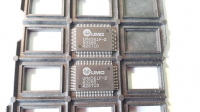
I have spare UM6561 for testing
Image Image

and there is direct connection only between those GND pins: 73, 60, 16.

Other pins marked as GND or NC in this schematics (32, 18, 19) might act as input pins. There is high probability of it, as multimeter on diode test shows some value for EACH of those pins with respect to GND, so they are internally connected.
Re: Schematic for UM6561?
by on (#203351)
The datasheet that Farid found for the UM6561 says that pin 19 is P1 D2 (i.e. famicom microphone).

I notice that he switched pin 32 from ground (in the initial pinout) to 5V (in his very first breadboarded picture, pin 32 is labelled "GND 5V")
Re: Schematic for UM6561?
by on (#203364)
Quote:
The datasheet that Farid found for the UM6561 says that pin 19 is P1 D2 (i.e. famicom microphone).

If it is Famicom microphone should I connect it GND (as suggested in Russian schematic) or leave it floating?

Quote:
I notice that he switched pin 32 from ground (in the initial pinout) to 5V (in his very first breadboarded picture, pin 32 is labelled "GND 5V")

It is definitely mislabeled in the Russian schematic since it is connected to other VCC pins internally.

And here is something interesting :
Quote:
跟据文章描述,改N制只要把晶振换成21.47727MHz就行了。

Google translate :
Quote:
According to the article described, change the N system as long as the crystal into 21.47727MHz on the line.
Re: Schematic for UM6561?
by on (#203367)
I confirm, pin 32 is connected to VCC. So out of those mysterious pins, only 18 is unknown, so it is probably pal/ntsc select.
Re: Schematic for UM6561?
by on (#203373)
FARID wrote:
If [pin 19] is [P1 D2] Famicom microphone should I connect it GND (as suggested in Russian schematic) or leave it floating?
Either's fine.


Google OCRs the first two paragraphs of the data sheet as
Quote:
在众多的中英电脑学习机中,用6561芯片开发出来的学习
机,可谓品牌众多。如“科王926”,“声霸”,“小霸王”,“小博士”
等,目前该芯片构成的学习机维修资料很少,本人从事UM6561
芯片的开发,维修多年,近一年又维修了一些中英文电脑学习
机,现将维修资料和检修实例整理出来与同行共享.

目前国内销售的UM6561集成块是UM6561 PAL / NTSC,
该芯片用26.601712MHz的晶振时,视频输出PAL彩色信号,
当使用21.47727MHz的晶振时,视频输出NTSC彩色电视信
号,这类中英文学习机在型号升级时(如486型到926型)从硬
件上看没有实质性的改变. 大多都是增加新的软件功能,也就是
学习卡中内容不同.
It does sound like it autodetects crystal frequency and switches between NTSC and Dendy behavior accordingly.
Re: Schematic for UM6561?
by on (#207256)
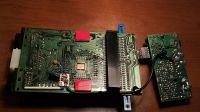
I just got one famiclone with glob-top UM6561 (soldered on add-on board), but there is also place for regular 80 pin SMD UM6561. What is weird, its pinout it shifted from original UM6561 (this pin1 = UM6561 pin2, this pin 2 = UM6561 pin3).

Image

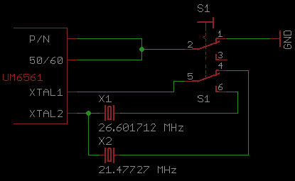
This board uses 26.601712 MHz crystal and has place for two jumpers - one marked as P/N and the other 50/60 (both were unsoldered, but soldering shorted each of them to GND).

Shorting P/N causes PAL screen to momentally switch to black/white, shorting 50/60 causes TV to lose sync (it is responsible for crystal selection).

So I did this clever switch and now I can in runtime switch between PAL and NTSC - curiously switching crystal during runtime does not cause CPU to break.
Image
I was worried if connecting crystal with only one leg and putting second leg on long wire and switch will have problems, but nothing that happened!
Re: Schematic for UM6561?
by on (#218192)
sorry to resurrect an old thread, @krzysiobal does what you did work with a UM6561f-2? i have 2 game axe color, both in need of a um6561cf-1 both failed. but i got some um6561f-2 that only work with pal xtal, and run terrible. i want NTSC! could you advise me? which pins on the umc package are affected by what you did? or what pins need to connect? BTW im a fan of your pcb and repro work! want to buy some soon!
Re: Schematic for UM6561?
by on (#218223)
I have just done some test using my IQ502, UM6561CF-2 based famiclone console (with 26.601712 MHz chip):
1. Replacing the crystal with 21.47727 MHz causes TV lose sync and slower sound, so the chip does NOT have region crystal audo detect frequency
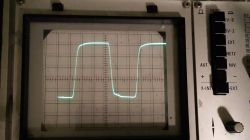
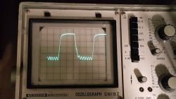
2. Pin 18 is NOT cabaple of switching region between PAL/NTSC. It is some kind of input (with itnernal pull-up to 5V), but when you apply 0V on it, console automatically hangs up. When you look on the scope at the M2 line when pin 18 is at 5V (or not connected to anything):
Image

and when it is tied to 0V:
Image

It seems to change the M2 appearance bit, but its further meaning is unknown.

3. Few weeks ago I had console also based on UM6561F-2 which had 21.47727 MHz crystal and was NTSC mode. Pin 18 was also not connected to anything, so probably the whole chip has the PAL/NTSC region set during the manufacturing process (and thats why some of them have UM6561BF / F / -1 / -2 markings)

So if you want to have PAL/NTSC switchable console, you need to obtain some glob-top clone with ability to add switch button.
Re: Schematic for UM6561?
by on (#218273)
Krzy, Thank you, that's EXACTLY what i thought and what i had observed. i installed a F-2 in my game axe to verify the board was fine and it was the NOAC that failed, and I could only get video with the 26mhz xtal. I've got a lead on some UM6561cf-1 from hong kong. looks like im going to have to shell out 25 usd per IC. Im ordering 5 in case of a failure in the future as i have 2 game axes with noac ram that failed due to poor ESD protection in the stock circuit. the 6561F-2 seems to be had for much cheaper, but i just can't adjust to Dendy PAL... lol
Re: Schematic for UM6561?
by on (#218350)
Any idea if these NOACs would work fine with 3.3v parts and not have problems in the future?
Re: Schematic for UM6561?
by on (#224221)
krzysiobal wrote:
I just got one famiclone with glob-top UM6561 (soldered on add-on board), but there is also place for regular 80 pin SMD UM6561. What is weird, its pinout it shifted from original UM6561 (this pin1 = UM6561 pin2, this pin 2 = UM6561 pin3).

Image

This board uses 26.601712 MHz crystal and has place for two jumpers - one marked as P/N and the other 50/60 (both were unsoldered, but soldering shorted each of them to GND).

Shorting P/N causes PAL screen to momentally switch to black/white, shorting 50/60 causes TV to lose sync (it is responsible for crystal selection).


Could you please show more photos of this board, from all sides? Also a photo of the famiclone itself also would be useful.