Starting a more in depth conversation about an idea I recently shared in discussion on methods for parallax techniques.
So the CIC is the 'necessary evil' of a ~50cent chip that must be included on any game seeking to be published in 72pin form. The current popular choice is the attiny13, selected by both Jim's cool and Krikzz. They utilize the 4Mhz CIC clock as the mcu's clock source and instruction cycle counting to ensure proper timing of communications with the main board CIC lock. The selection of the attiny13 is a rather easy choice to target for a CIC solution. It effectively the lowest cost microchip (AVR/PIC) solution that has adaquate i/o and nvm to store the current region.
For several different NES/SNES projects I've been considering an alternate CIC solution that might allow the 50cent budget of the CIC to go towards a more powerful chip that would be capable of being dual tasked with CIC comms and some sort of mapper interfacing. The attiny13 doesn't really have the io nor time to spare for dual tasking.
Looking over Krikzz's implemenation after the first few cycles where the current stream is determined, the main loop spins for 260+ cycles (65 usec) between each Din/Dout transaction. I took some quick logic analyzer captures to confirm there is ~75usec between each transaction. So the attiny13 operating at 4Mhz is only spending ~15% of it's time processing CIC communications. With not other mcu timers available and nothing better to do with it's time the attiny13 has no choice other than cycle counting. Trying to make use of the 2 remaining i/o, during that under utilized time would be rather challenging with exact cycle counting and not options for interrupts etc.
So I started entertaining the idea of other chips available on the market. For this purpose I discounted all other microchip offerings as they will be more expensive than the attiny13. With those options discounted, and only the requirement of 5v supply and NVM/eeprom available there are a couple interesting options.
Cypress's CY8C4013SXI-400 is an interesting option with it's 16Mhz cortex M0, but only has 5io. I'm tempted to target it considering it's cheaper than the attiny13 in volume, but the lack of spare i/o significantly limits what's possible. The recent SROM cracking that might double the flash for free is an interesting bonus however..
The two most interesting prospects I found were STM offerings. The STM32F030F4 with it's 48Mhz cortex M0 was quoted to me with better pricing than the attiny13. Even though it's a 3v part, it has enough 5v tolerant i/o to get the CIC job done. This is a nice option for a cartridge with 3v mapper logic. And the 48Mhz M0 certainly has enough power to have only a small portion of it's time consumed by CIC communications. I'm still kind of interested in tasking one of the STM32F0 family parts with both CIC and mapper tasks. But for the purpose of this conversation, it's not a viable solution due to too few 5v tolerant io.
That brings me to what I've deemed the 'winner' of the STM8S003F4 datasheet here
It's a rather basic 8 bit mcu with common features including:
This all comes at a significant price drop compared to the attiny13 in volume. The price alone is enough to motivate me to create my own CIC implementation using the STM8. But there's a considerable amount of extra hardware getting left unused if only tasked to be a CIC. If only being tasked as a CIC the easilest solution would probably be to clock the mcu externally by the 4Mhz CIC clock. Then implement the CIC in much the same method that the attiny13 did. But that's not much fun, and I think I can do better than that.
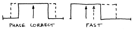
My goal is to run at 16Mhz and use one of the timers to interrupt the mcu every ~75usec to handle the next CIC transaction. Doing that means the CIC CLK signal is pretty useless. But one would have to take care to keep aligned with the CIC's clock. The interrupt would have to come early and maybe poll the Din pin when it's expected to be high to sense how far the mcu has drifted and correct it's internal timer. I'm expecting that worst case 15usec out of every 75usec will be utilized for CIC transfers. That's more time than Krikzz is utilizing with the attiny13, and we're running 4x faster. Maybe this solution could get to 5usec or less, either way it doesn't matter too much, it's still some portion of time the mcu MUST prioritize CIC transfers.
Now comes the question of if this extra hardware is going to be utilized by the NES somehow, the CPU has to have a means to interface with the mcu. This is not a simple feat with the expectation of being free. I argued to myself that all the hoops that would need to be jumped through would make disinterest one to the point where you'd want to simply invest a couple dollars on a mapper more capable than a discrete mapper.
Here's the pinout and port numbering with some preliminary assignments I've came up with:
The simplest method I could come up with would be to designate an unused mapper register bit to have the NES signal/interupt the mcu that it wants it's attention to start communicating to it. However this mcu interrupt must have a lower priority than CIC comms. Assuming a '377 is being used for the mapper reg we probably have an unused bit, even a BNROM utilizing a '161 has a unused bit if the PRG-ROM is <= 256KByte.
When the mapper bit is set (presumably $8000.7) the mcu would be instructed to start listening to CPU writes when CPU A13 is high. This maps mcu's register to $6000-7FFF, but also maps/overlaps the PPU $2000-3FFF. This was the fewest number of pins I could come up with for decoding that seems reasonable. Moving the mcu reg bits to SPI's PC bits would give more bits for decoding and potentially decoding CPU A14 perhaps. But A13 seems sufficient as it blocks writes to RAM and the APU which seems helpful to me. The user would have to take care to not accidentally write to the PPU and mcu at the same time, but one should already be very deliberate when writing to the PPU.
My proposed pin assignments would allow for 4bit nibble wide read/writes at a minimum. If one wasn't looking to utilize the UART then the entirety of PORT D could be used for 6bit wide accesses.
There is a problem though as we can't be certain the mcu is always able to listen to writes to $6000. The mcu could be currently interrupted by CIC comms which must have a higher priority. I can't think of a very clean way to get around this without adding dedicated logic. Maybe the simplest idea is to have the NES set the mcu interrupt bit $8000.7, then the mcu waits for upcoming CIC comm to complete. Once done, it interupts the NES CPU which uses it's interrupt routine to complete the transfer. The NES would have the maximum time (~60usec) to complete the transfer. This is probably a preferred solution if the NES CPU is looking to make big transfers to the mcu. Maybe a big transfer would be verified by reading back a checksum.
Another idea might be to write to $6000, but require the value to be read back from the mcu before being certain it stuck. This would probably be a preferred solution for small transfers as we typically have >80% chance the mcu is listening.
You could maybe combine the two ideas to remove the need to use NES /IRQs for each transfer. Maybe the NES can simply read from the mcu at $6000 after setting the $8000.7 mcu interupt bit. And the mcu provides a designated value if there is sufficent time to write a nibble or two before the next CIC xfr.
Anyway, that's my idea and here's the place to toss out any other probably better ideas you guys might have. My primary goal for such an interface is that it's effectively free being able to be implemented with wires alone. It's not out of the question to add logic gates to implement the idea, but personally I'm not interested in doing so. Start adding a gate here or there and it's no longer free. I'm not even sure I have the pcb space currently to support routing the signals I've proposed. I'll probably have to re-route a large portion of my current design to make room for the CIC to be placed closer to the PRG side of the board.
As far as ideas of what could be done with utilization of something like this it's up to the imagination. The mcu probably isn't going to be fast enough to implement any sort of CHR effects like finer backswitching or anything. Even permitting selectable NT mirroring is sorta out of the question as you'd need to add more logic.
As mentioned in my other post, unfortunately this mcu doesn't have any external pins available to clock the internal counters. So you'd have to utilize the internal 16Mhz/128Khz oscillators for an IRQ timer. The SPI bus is open on my pinout proposal above, and things could be shifted around to make the I2C bus available instead. This potentially be connected to a large serial flash rom for lots of rom storage. But it's not going to be as fast as one might like due to the limitations put on transfers. One of the pins could be routed to EXP6 to implement some basic expansion sound perhaps. You could even get crazy and utilize the UART interface to connect a cheapo BT/WiFi module, but if you're interested in that doesn't make much sense to restrict your budget to a discrete mapper..
Anyway, my guess is chances are this idea won't go anywhere, but it's fun to talk about. At this point I can say I'm going to do everything I can to migrate to the STM8 for my NES/SNES CIC solutions for the benefit of my other designs. So from that point the hardware will be sitting idle waiting to be put to good use.
So the CIC is the 'necessary evil' of a ~50cent chip that must be included on any game seeking to be published in 72pin form. The current popular choice is the attiny13, selected by both Jim's cool and Krikzz. They utilize the 4Mhz CIC clock as the mcu's clock source and instruction cycle counting to ensure proper timing of communications with the main board CIC lock. The selection of the attiny13 is a rather easy choice to target for a CIC solution. It effectively the lowest cost microchip (AVR/PIC) solution that has adaquate i/o and nvm to store the current region.
For several different NES/SNES projects I've been considering an alternate CIC solution that might allow the 50cent budget of the CIC to go towards a more powerful chip that would be capable of being dual tasked with CIC comms and some sort of mapper interfacing. The attiny13 doesn't really have the io nor time to spare for dual tasking.
Looking over Krikzz's implemenation after the first few cycles where the current stream is determined, the main loop spins for 260+ cycles (65 usec) between each Din/Dout transaction. I took some quick logic analyzer captures to confirm there is ~75usec between each transaction. So the attiny13 operating at 4Mhz is only spending ~15% of it's time processing CIC communications. With not other mcu timers available and nothing better to do with it's time the attiny13 has no choice other than cycle counting. Trying to make use of the 2 remaining i/o, during that under utilized time would be rather challenging with exact cycle counting and not options for interrupts etc.
So I started entertaining the idea of other chips available on the market. For this purpose I discounted all other microchip offerings as they will be more expensive than the attiny13. With those options discounted, and only the requirement of 5v supply and NVM/eeprom available there are a couple interesting options.
Cypress's CY8C4013SXI-400 is an interesting option with it's 16Mhz cortex M0, but only has 5io. I'm tempted to target it considering it's cheaper than the attiny13 in volume, but the lack of spare i/o significantly limits what's possible. The recent SROM cracking that might double the flash for free is an interesting bonus however..
The two most interesting prospects I found were STM offerings. The STM32F030F4 with it's 48Mhz cortex M0 was quoted to me with better pricing than the attiny13. Even though it's a 3v part, it has enough 5v tolerant i/o to get the CIC job done. This is a nice option for a cartridge with 3v mapper logic. And the 48Mhz M0 certainly has enough power to have only a small portion of it's time consumed by CIC communications. I'm still kind of interested in tasking one of the STM32F0 family parts with both CIC and mapper tasks. But for the purpose of this conversation, it's not a viable solution due to too few 5v tolerant io.
That brings me to what I've deemed the 'winner' of the STM8S003F4 datasheet here
It's a rather basic 8 bit mcu with common features including:
- 16Mhz & 128Khz internal RC oscillators
- 8KByte flash, 1Kbyte SRAM, 128Byte eeprom
- Nested vector interupt controller including external interrupts
- 2x 16bit adv/gen purp counters, 1x 8bit basic counter
- 16x GPIO
- UART, SPI, I2C interfaces
This all comes at a significant price drop compared to the attiny13 in volume. The price alone is enough to motivate me to create my own CIC implementation using the STM8. But there's a considerable amount of extra hardware getting left unused if only tasked to be a CIC. If only being tasked as a CIC the easilest solution would probably be to clock the mcu externally by the 4Mhz CIC clock. Then implement the CIC in much the same method that the attiny13 did. But that's not much fun, and I think I can do better than that.
My goal is to run at 16Mhz and use one of the timers to interrupt the mcu every ~75usec to handle the next CIC transaction. Doing that means the CIC CLK signal is pretty useless. But one would have to take care to keep aligned with the CIC's clock. The interrupt would have to come early and maybe poll the Din pin when it's expected to be high to sense how far the mcu has drifted and correct it's internal timer. I'm expecting that worst case 15usec out of every 75usec will be utilized for CIC transfers. That's more time than Krikzz is utilizing with the attiny13, and we're running 4x faster. Maybe this solution could get to 5usec or less, either way it doesn't matter too much, it's still some portion of time the mcu MUST prioritize CIC transfers.
Now comes the question of if this extra hardware is going to be utilized by the NES somehow, the CPU has to have a means to interface with the mcu. This is not a simple feat with the expectation of being free. I argued to myself that all the hoops that would need to be jumped through would make disinterest one to the point where you'd want to simply invest a couple dollars on a mapper more capable than a discrete mapper.
Here's the pinout and port numbering with some preliminary assignments I've came up with:
Code:
_________________ _______________
NES CPU D3 -| PD4/UART_CLK \/ PD3 |- CPU D2
NES CPU D4/UART TX -| PD5/UART_TX PD2 |- CPU D1
NES CPU D5/UART RX -| PD6/UART_RX ISP/PD1 |- CPU D0
-| /RST MISO/PC7 |- SPI?
MAPPER REG BIT -| PA1/OSCIN MOSI/PC6 |- SPI?
CIC Din -| PA2/OSCOUT SCK/PC5 |- SPI?
-| VSS PC4 |- NES /IRQ
-| Vcap PC3 |- CIC Dout?
-| VDD SCL/PB4 |- NES CPU R/W
SPI? CICrst? -| PA3/SPI_NSS SDA/PB5 |- NES A13
---------------------------------
The simplest method I could come up with would be to designate an unused mapper register bit to have the NES signal/interupt the mcu that it wants it's attention to start communicating to it. However this mcu interrupt must have a lower priority than CIC comms. Assuming a '377 is being used for the mapper reg we probably have an unused bit, even a BNROM utilizing a '161 has a unused bit if the PRG-ROM is <= 256KByte.
When the mapper bit is set (presumably $8000.7) the mcu would be instructed to start listening to CPU writes when CPU A13 is high. This maps mcu's register to $6000-7FFF, but also maps/overlaps the PPU $2000-3FFF. This was the fewest number of pins I could come up with for decoding that seems reasonable. Moving the mcu reg bits to SPI's PC bits would give more bits for decoding and potentially decoding CPU A14 perhaps. But A13 seems sufficient as it blocks writes to RAM and the APU which seems helpful to me. The user would have to take care to not accidentally write to the PPU and mcu at the same time, but one should already be very deliberate when writing to the PPU.
My proposed pin assignments would allow for 4bit nibble wide read/writes at a minimum. If one wasn't looking to utilize the UART then the entirety of PORT D could be used for 6bit wide accesses.
There is a problem though as we can't be certain the mcu is always able to listen to writes to $6000. The mcu could be currently interrupted by CIC comms which must have a higher priority. I can't think of a very clean way to get around this without adding dedicated logic. Maybe the simplest idea is to have the NES set the mcu interrupt bit $8000.7, then the mcu waits for upcoming CIC comm to complete. Once done, it interupts the NES CPU which uses it's interrupt routine to complete the transfer. The NES would have the maximum time (~60usec) to complete the transfer. This is probably a preferred solution if the NES CPU is looking to make big transfers to the mcu. Maybe a big transfer would be verified by reading back a checksum.
Another idea might be to write to $6000, but require the value to be read back from the mcu before being certain it stuck. This would probably be a preferred solution for small transfers as we typically have >80% chance the mcu is listening.
You could maybe combine the two ideas to remove the need to use NES /IRQs for each transfer. Maybe the NES can simply read from the mcu at $6000 after setting the $8000.7 mcu interupt bit. And the mcu provides a designated value if there is sufficent time to write a nibble or two before the next CIC xfr.
Anyway, that's my idea and here's the place to toss out any other probably better ideas you guys might have. My primary goal for such an interface is that it's effectively free being able to be implemented with wires alone. It's not out of the question to add logic gates to implement the idea, but personally I'm not interested in doing so. Start adding a gate here or there and it's no longer free. I'm not even sure I have the pcb space currently to support routing the signals I've proposed. I'll probably have to re-route a large portion of my current design to make room for the CIC to be placed closer to the PRG side of the board.
As far as ideas of what could be done with utilization of something like this it's up to the imagination. The mcu probably isn't going to be fast enough to implement any sort of CHR effects like finer backswitching or anything. Even permitting selectable NT mirroring is sorta out of the question as you'd need to add more logic.
As mentioned in my other post, unfortunately this mcu doesn't have any external pins available to clock the internal counters. So you'd have to utilize the internal 16Mhz/128Khz oscillators for an IRQ timer. The SPI bus is open on my pinout proposal above, and things could be shifted around to make the I2C bus available instead. This potentially be connected to a large serial flash rom for lots of rom storage. But it's not going to be as fast as one might like due to the limitations put on transfers. One of the pins could be routed to EXP6 to implement some basic expansion sound perhaps. You could even get crazy and utilize the UART interface to connect a cheapo BT/WiFi module, but if you're interested in that doesn't make much sense to restrict your budget to a discrete mapper..
Anyway, my guess is chances are this idea won't go anywhere, but it's fun to talk about. At this point I can say I'm going to do everything I can to migrate to the STM8 for my NES/SNES CIC solutions for the benefit of my other designs. So from that point the hardware will be sitting idle waiting to be put to good use.
 .
. 