I need some kind of advice. My FPGA dev-cart needs M2 signal for clocking internal circuitries, but also for decoding accessess to $6000-$7fff (and also $4000-$5fff as some mappers, eg. mapper 90 uses this).
I know there is a delay of tens of nanoseconds between M2 changes and !ROMSEL changes
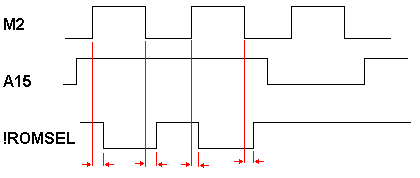
so M2 transitions need to be delayed by that time.
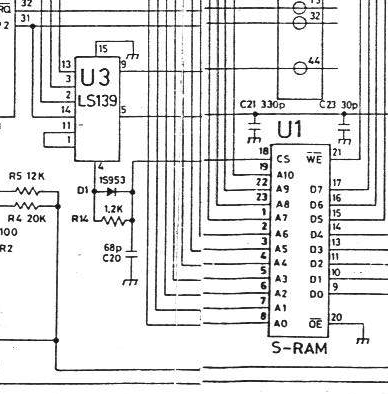
There is lidnariq's proposition at the wiki:
which in my opinion needs adding diode (the diode should be drawn backwards, sorry):
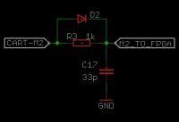
because only rising edges on M2 need to be delayed. That is because all data & address latching into FPGA on CPU writes occurs at falling edge of M2, because that is the time the data is valid (at rising edge of m2 data is not valid). Anyway, never mind.
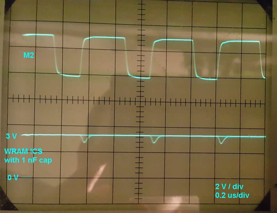
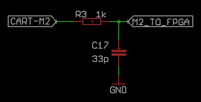
From my testing on various famiclones I figured out that 30pF is enough for most famiclones, but not for all - around 80 pF does the job. (otherwise writing to $E000-$FFFF causes data corruption in RAM mapped at $6000-$7FFFF.) Unfortunately, my FPGA has 3.3V IO pins so I had to put the `delayed` M2 thru 74LVC245 5V->3.3V converter. Unfortunately, this chip has maximum of 10ns/V rising time
 .
.
What does that mean? With R*C = 1 kOhm * 28 pF the rising time at its slowest point is around 9 ns/V which is OK - and the output signal is OK.
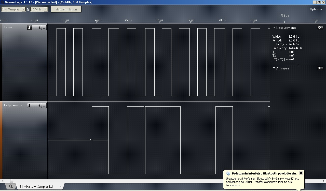
When I increase C to 96 pF, the rising time becomes 32 ns which is too much. Too slow rising time makes various metastable states inside the 74lvc245 which makes its output behave weird - probably quick glitches are observed. Neither my analog scope nor my logic analyzer was able to see those glitches, but when I clock my FPGA with that signal, it detect those glitches. For exaample - when I clock my FPGA with that signal and I force it to change output signal on each of clock rising edge, I got something like that, instead of just M2 x 2.

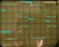
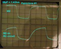
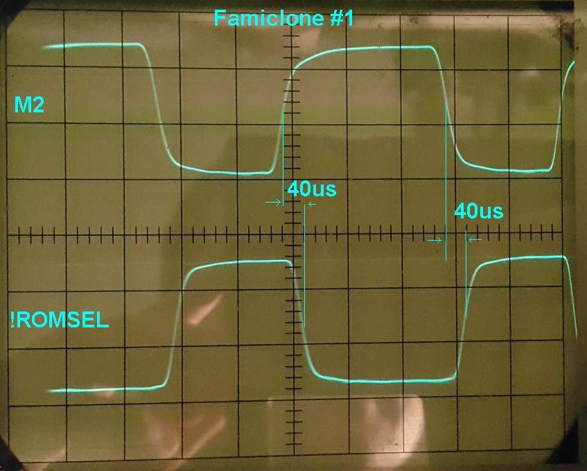
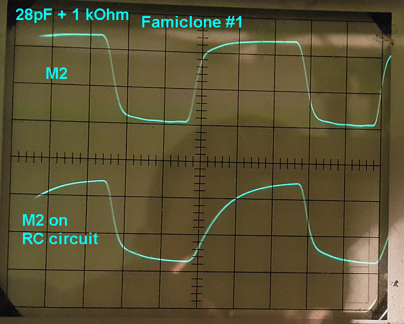
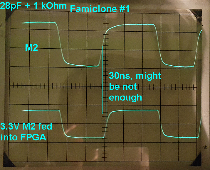
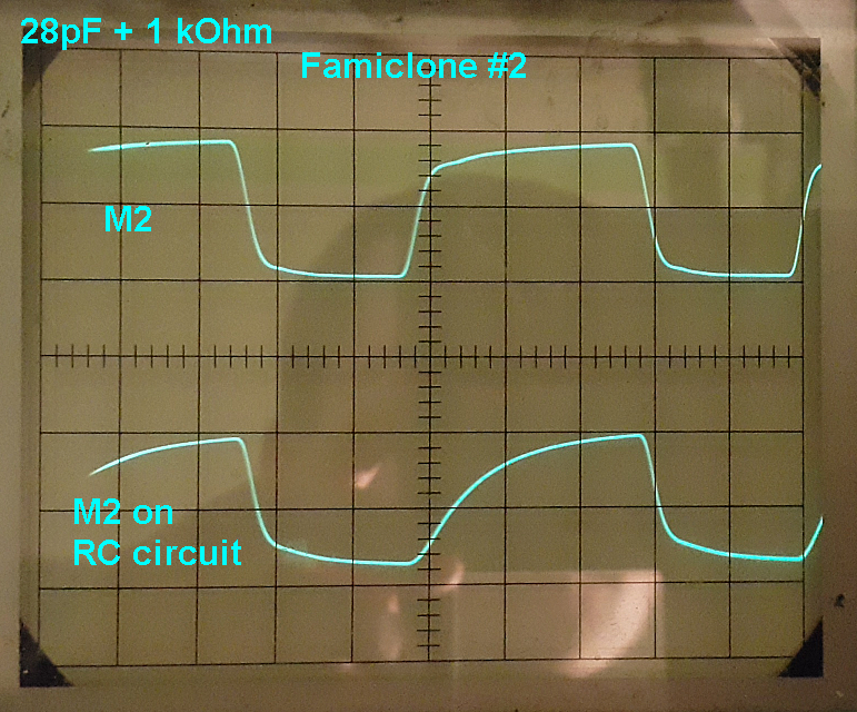
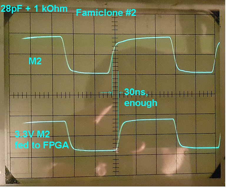
Here are some waveforms - all 2V/div, 0.1us/div
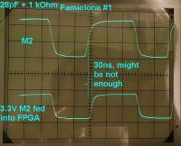
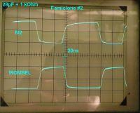
First - I tested with 28 pF.
Famiclone #1 (this one has longer !ROMSEL delay - about 40 ns) - 28 pF might be not enough:
Famiclone #2 (this one has shorter !ROMSEL delay - about 30 ns) - 28pF should be ok:
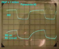

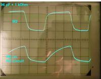
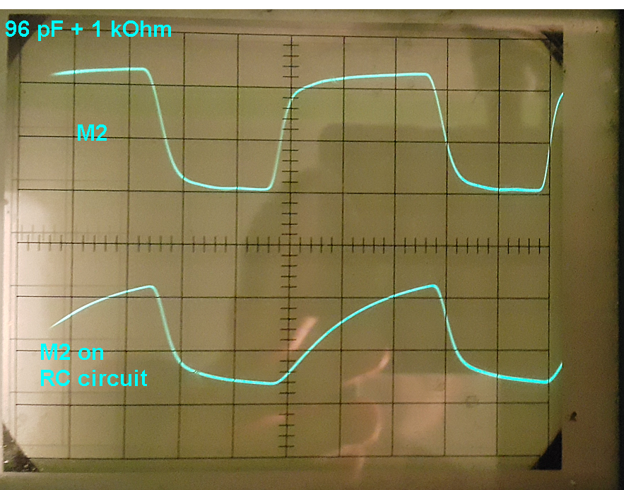
And just for curiosity - shape of M2 on RC circuit when 96 pF.
First solution would be just fed to FPGA two signals - one not delayed M2 for clocking purposes, and secod glitched and delayed M2 for restoring A15 and thus decoding PRG-RAM, etc.
Second solution is to use schmitt on delayed M2 signal, before puting in on 74lvc245, but i dont want to use additional chips.
The FPGA has built-in schmitt trigger inputs, but it's useless at this purpuse because signal on 74lvc245 is not slow rising, but glitched.
Do you have any other idea how to use just one delayed M2 for all purposes in FPGA?
I know there is a delay of tens of nanoseconds between M2 changes and !ROMSEL changes
so M2 transitions need to be delayed by that time.
There is lidnariq's proposition at the wiki:
which in my opinion needs adding diode (the diode should be drawn backwards, sorry):
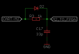
because only rising edges on M2 need to be delayed. That is because all data & address latching into FPGA on CPU writes occurs at falling edge of M2, because that is the time the data is valid (at rising edge of m2 data is not valid). Anyway, never mind.
From my testing on various famiclones I figured out that 30pF is enough for most famiclones, but not for all - around 80 pF does the job. (otherwise writing to $E000-$FFFF causes data corruption in RAM mapped at $6000-$7FFFF.) Unfortunately, my FPGA has 3.3V IO pins so I had to put the `delayed` M2 thru 74LVC245 5V->3.3V converter. Unfortunately, this chip has maximum of 10ns/V rising time
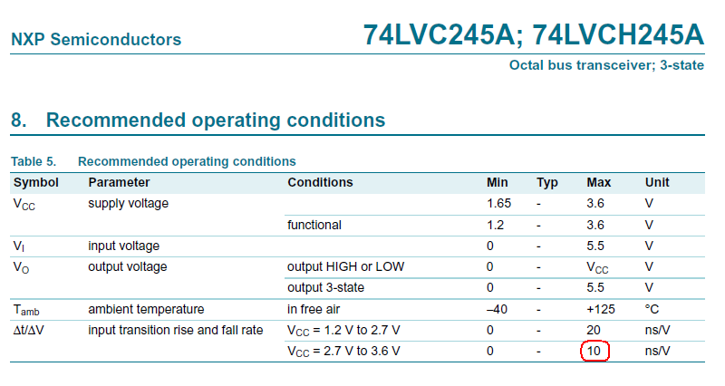 .
.What does that mean? With R*C = 1 kOhm * 28 pF the rising time at its slowest point is around 9 ns/V which is OK - and the output signal is OK.
When I increase C to 96 pF, the rising time becomes 32 ns which is too much. Too slow rising time makes various metastable states inside the 74lvc245 which makes its output behave weird - probably quick glitches are observed. Neither my analog scope nor my logic analyzer was able to see those glitches, but when I clock my FPGA with that signal, it detect those glitches. For exaample - when I clock my FPGA with that signal and I force it to change output signal on each of clock rising edge, I got something like that, instead of just M2 x 2.
Here are some waveforms - all 2V/div, 0.1us/div
First - I tested with 28 pF.
Famiclone #1 (this one has longer !ROMSEL delay - about 40 ns) - 28 pF might be not enough:
Famiclone #2 (this one has shorter !ROMSEL delay - about 30 ns) - 28pF should be ok:

And just for curiosity - shape of M2 on RC circuit when 96 pF.
First solution would be just fed to FPGA two signals - one not delayed M2 for clocking purposes, and secod glitched and delayed M2 for restoring A15 and thus decoding PRG-RAM, etc.
Second solution is to use schmitt on delayed M2 signal, before puting in on 74lvc245, but i dont want to use additional chips.
The FPGA has built-in schmitt trigger inputs, but it's useless at this purpuse because signal on 74lvc245 is not slow rising, but glitched.
Do you have any other idea how to use just one delayed M2 for all purposes in FPGA?