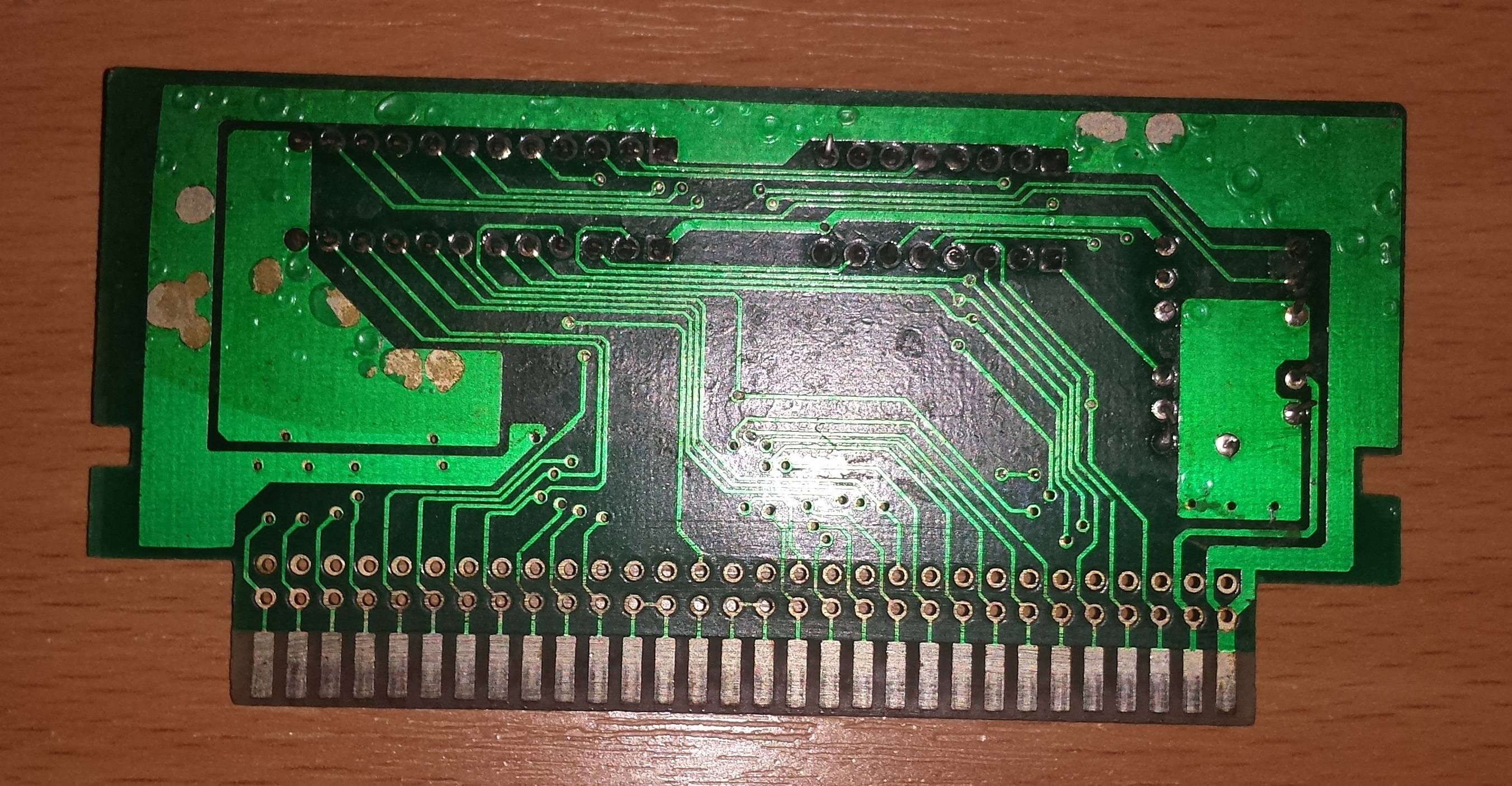
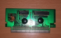
I am reverse engineering ASDER 20 in 1 multicart.
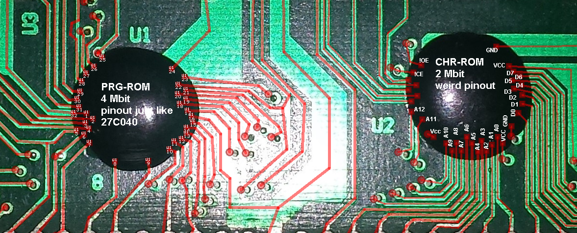
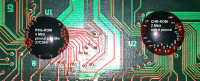
While the 4 Mbit PRG memory has pinout the same like 27c040, 2Mbit CHR has quite weird pinout. Do you know name of any eprom chip with same pinout?
While the 4 Mbit PRG memory has pinout the same like 27c040, 2Mbit CHR has quite weird pinout. Do you know name of any eprom chip with same pinout?