MMC5 on TTL components
I wanted to started this thread almost year ago, but I did not have enough patience to it. Now it's high time to come back to this topic as the cartridges that are subject of it are in my hands.
Most popular ASIC mappers have been replicated using discrete chips with more or less effort in pirate cartridges (bootlegs). Sometimes not all functionality has been replicated or game had to been modified.
For example:
MMC3: http://wiki.nesdev.com/w/index.php/INES_Mapper_106
FME7: http://wiki.nesdev.com/w/index.php/Pirate_FME7
MMC1
MMC2: https://forums.nesdev.com/viewtopic.php ... 30#p186157
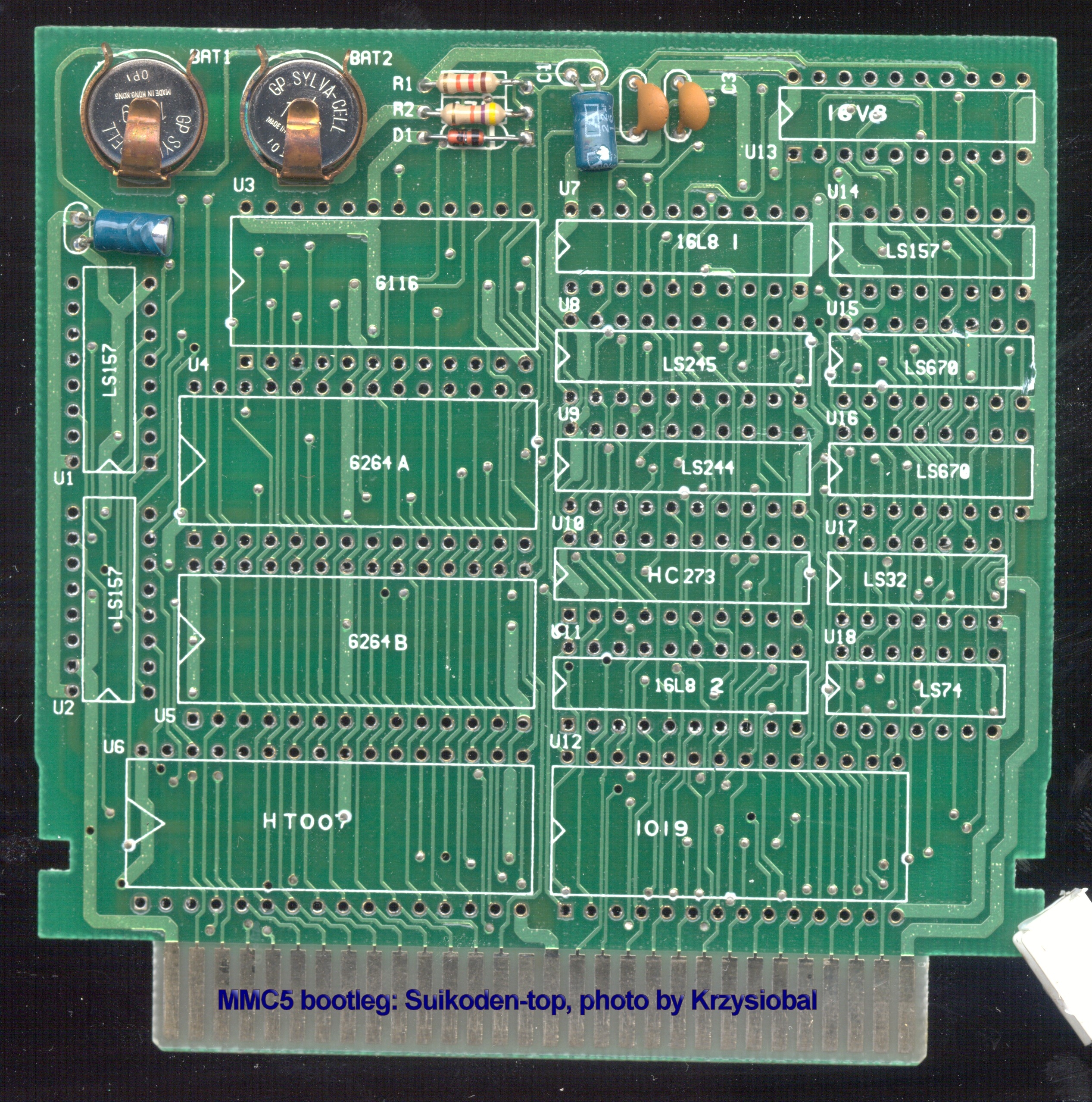
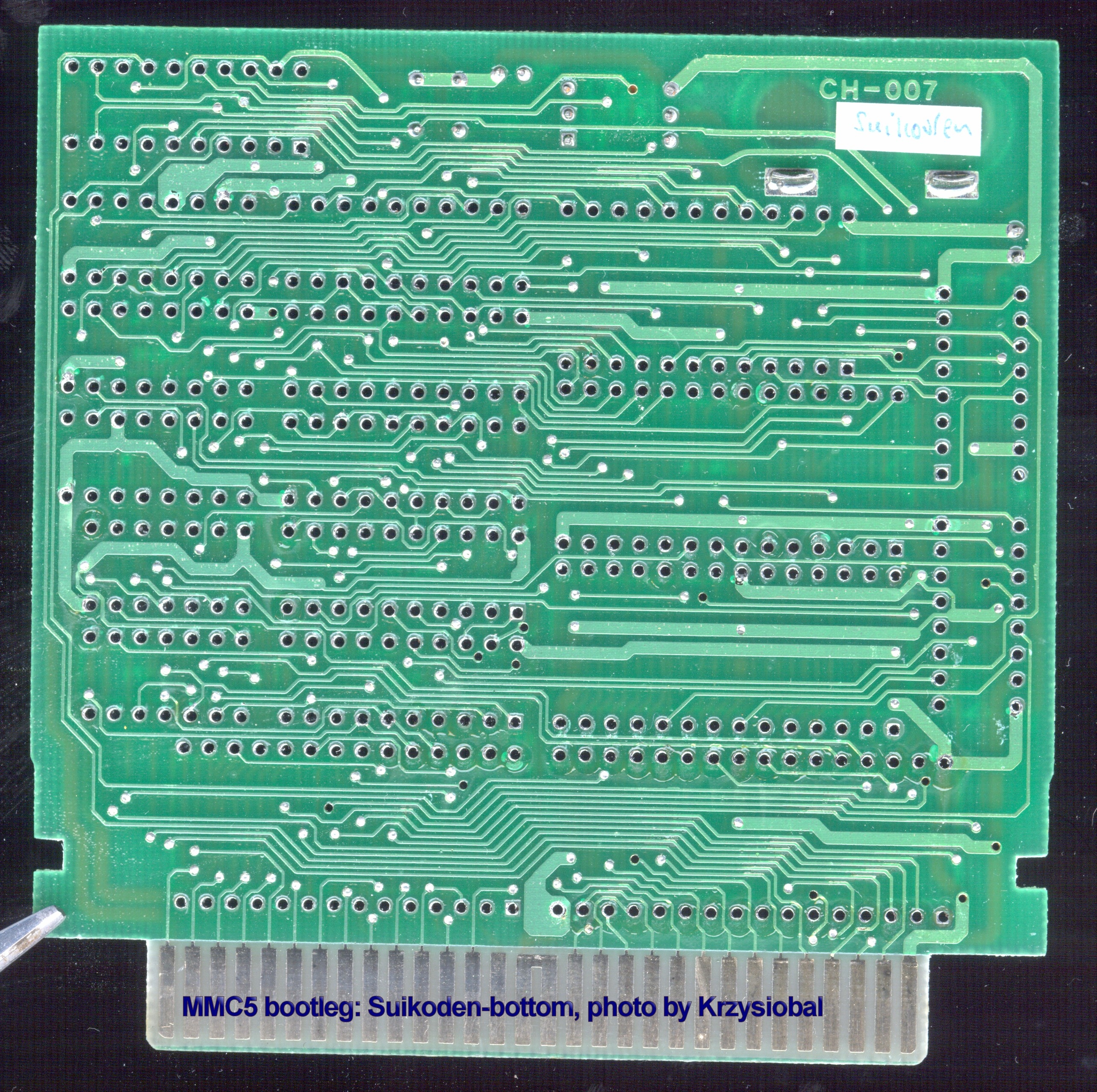
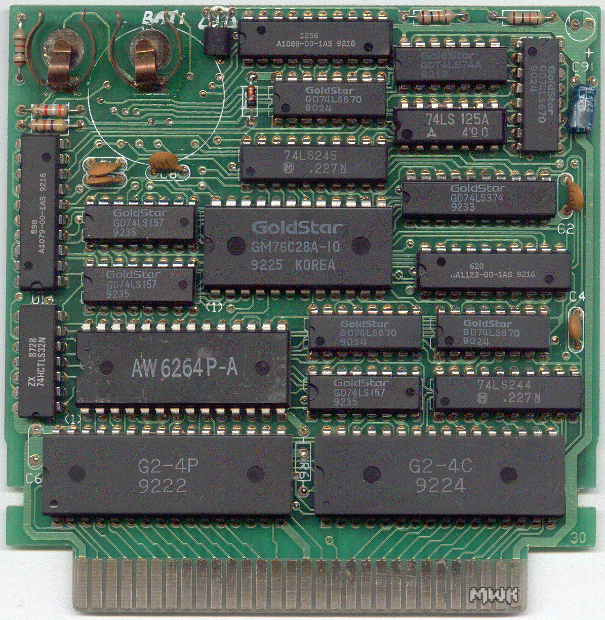
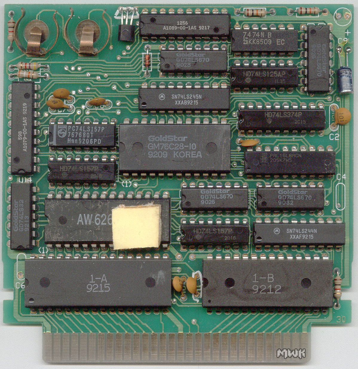
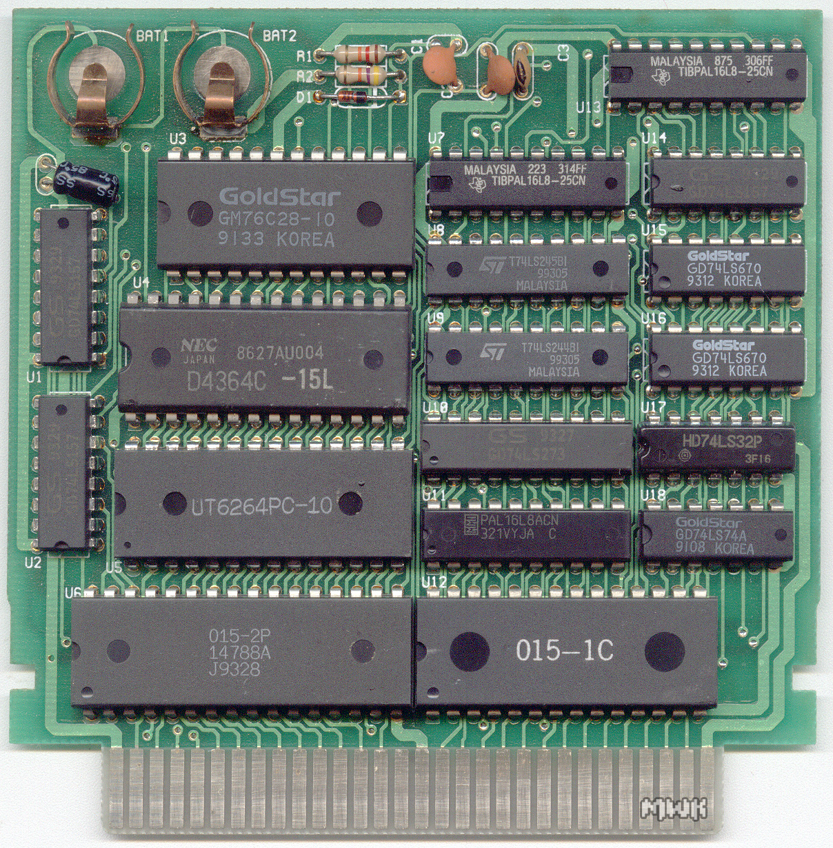
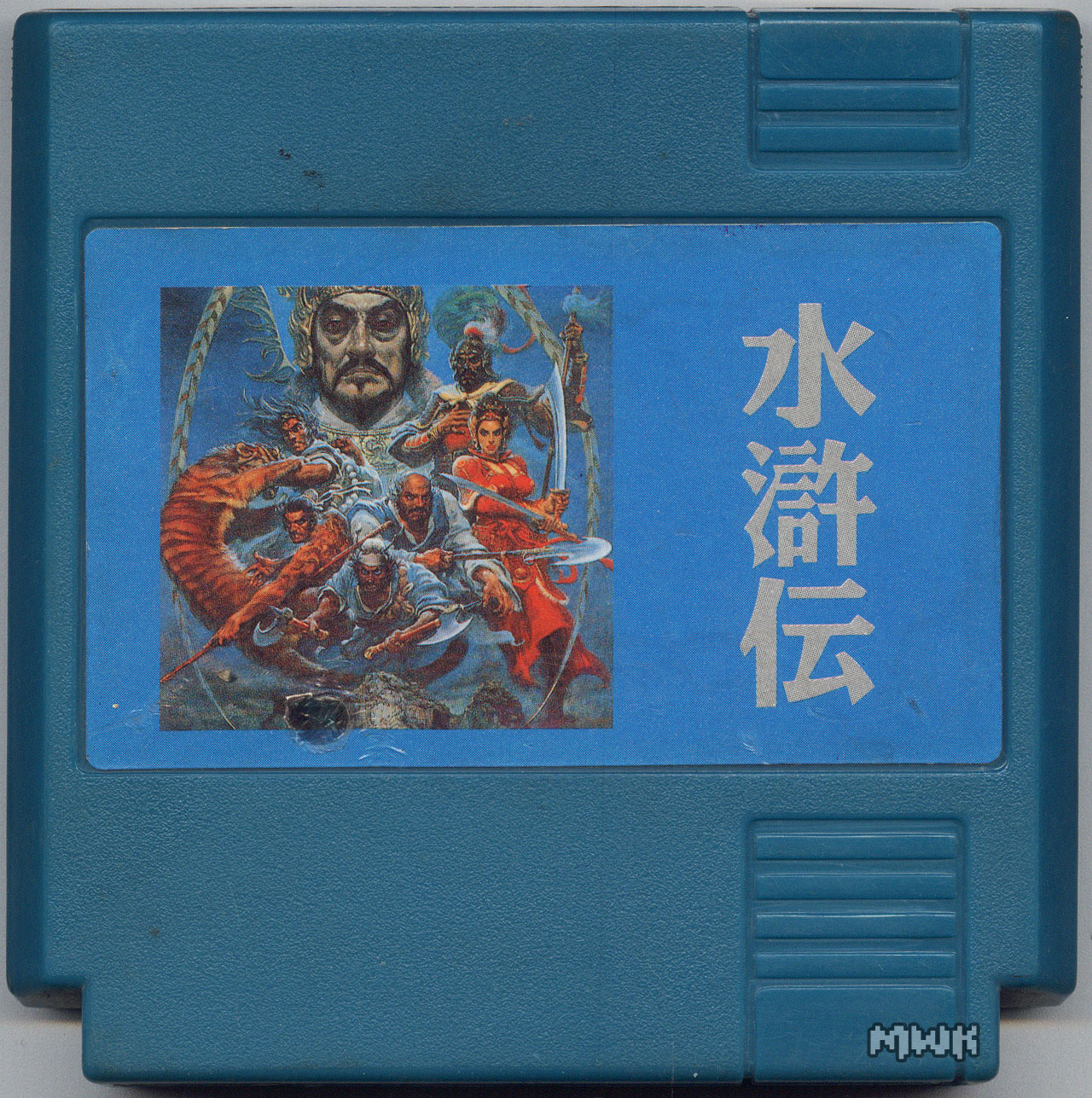
About year ago my friend shown me photos of MMC5 bootleg game - Sangokushi 2. It contained a lot of chips and 3 PALs. I reverse engineered the schematics and the friend tried to dump those pals using my advices. Unfortunately 1 of them had internal memory (output with feedback) and the friend was dumping it using regular programmer with pal connected as a memory - all I could do was just to suggest rearranging address lines for different dumping results. That did not lead to the solution so I was looking a year ago for this cart to become in my hands. Meanwhile this friend shown me another 2 bootleg MMC5 games: L'emperaur and Suikoden. While L`Emperaur has almost identical PCB to the Sangokushi 2 (with the exception that Sangokushi 2 has 256K DIP32 CHR-ROM and L`Emperaur has 128K DIP28), Suikoden has muchdifferent one.
Now I have both L`emperaur and Suikoden in my hands and I can finish the rev-eng process of them and creating description of mapper they use. It is not fully MMC5 - register addresses are different but some primary functionality (EX-RAM, fill-mode nametable) are present.
CHR is identical to the original release, PRG has some minor changes, for example: (:D)
I am really proud of examining those non-combinatorial outputs of PALs. For every non-combinatorial output there is one latch (which latches value at certain condition). Latched value is available at one of the unwired output. So the non-combinatorial output can be thought as a combinatorial function of other inputs and those latched values.
I don't know yet what PPU is doing every its clock cycle and this knowledge is crucial to understand how thee fill-mode works.
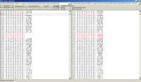
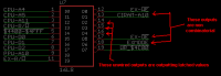
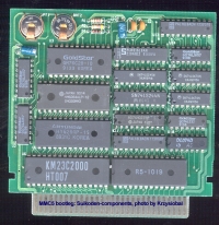
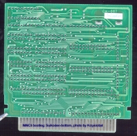
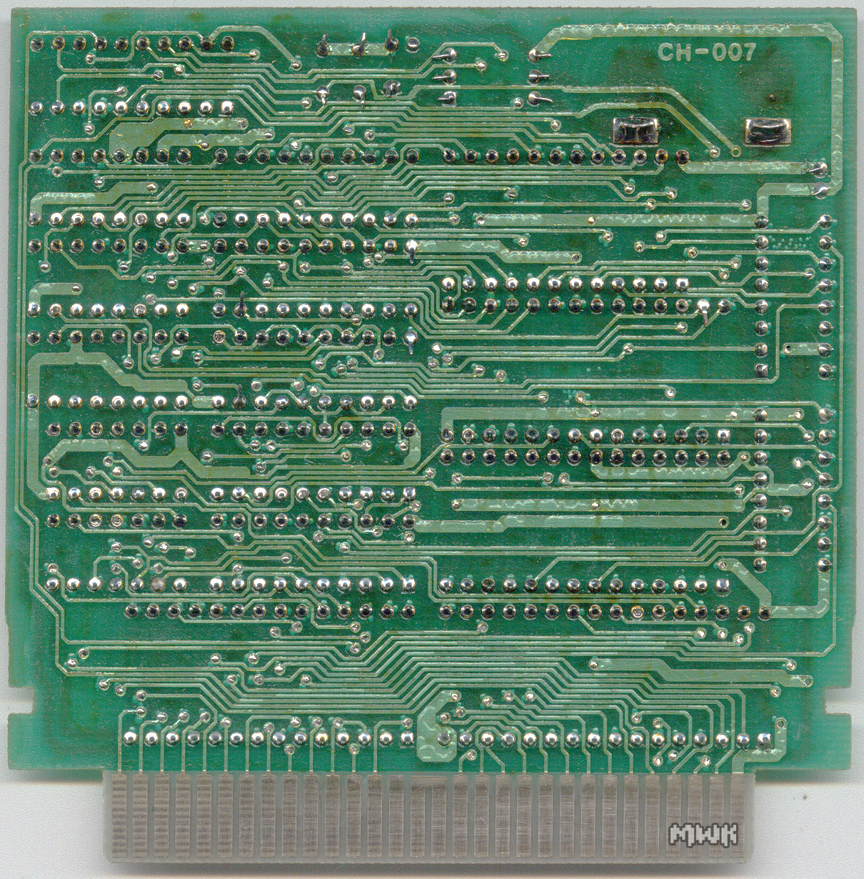
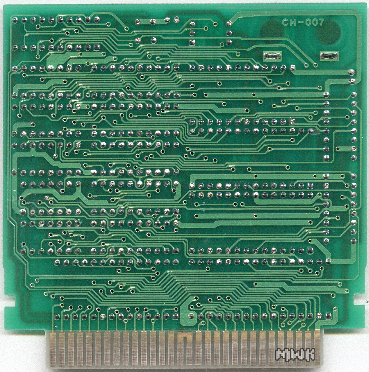
Here are photos and schematic:

Here are PAL details and mapper description I did so far
EX-RAM behaviour:
CPU has two windows ($5400-$57ff and $5c00-$5fff) to read/write to EX-RAM memory.
The behaviour of EX-RAM depends of how $4c30 bits are set.
CPU can always write to EX RAM (and those write cycles have priority over any other EXRAM activity)
0: reading from EXRAM (by CPU/PPU) returns open bus; CPU can write to EX-RAM.
1: reading EXRAM by CPU returns open bus; CPU can write to EX-RAM; PPU can read EX-RAM
2-3: CPU can read & write to EX-RAM, PPU cannot read from it.
I wanted to started this thread almost year ago, but I did not have enough patience to it. Now it's high time to come back to this topic as the cartridges that are subject of it are in my hands.
Most popular ASIC mappers have been replicated using discrete chips with more or less effort in pirate cartridges (bootlegs). Sometimes not all functionality has been replicated or game had to been modified.
For example:
MMC3: http://wiki.nesdev.com/w/index.php/INES_Mapper_106
FME7: http://wiki.nesdev.com/w/index.php/Pirate_FME7
MMC1
MMC2: https://forums.nesdev.com/viewtopic.php ... 30#p186157
About year ago my friend shown me photos of MMC5 bootleg game - Sangokushi 2. It contained a lot of chips and 3 PALs. I reverse engineered the schematics and the friend tried to dump those pals using my advices. Unfortunately 1 of them had internal memory (output with feedback) and the friend was dumping it using regular programmer with pal connected as a memory - all I could do was just to suggest rearranging address lines for different dumping results. That did not lead to the solution so I was looking a year ago for this cart to become in my hands. Meanwhile this friend shown me another 2 bootleg MMC5 games: L'emperaur and Suikoden. While L`Emperaur has almost identical PCB to the Sangokushi 2 (with the exception that Sangokushi 2 has 256K DIP32 CHR-ROM and L`Emperaur has 128K DIP28), Suikoden has muchdifferent one.
Now I have both L`emperaur and Suikoden in my hands and I can finish the rev-eng process of them and creating description of mapper they use. It is not fully MMC5 - register addresses are different but some primary functionality (EX-RAM, fill-mode nametable) are present.
CHR is identical to the original release, PRG has some minor changes, for example: (:D)

I am really proud of examining those non-combinatorial outputs of PALs. For every non-combinatorial output there is one latch (which latches value at certain condition). Latched value is available at one of the unwired output. So the non-combinatorial output can be thought as a combinatorial function of other inputs and those latched values.

I don't know yet what PPU is doing every its clock cycle and this knowledge is crucial to understand how thee fill-mode works.
Here are photos and schematic:

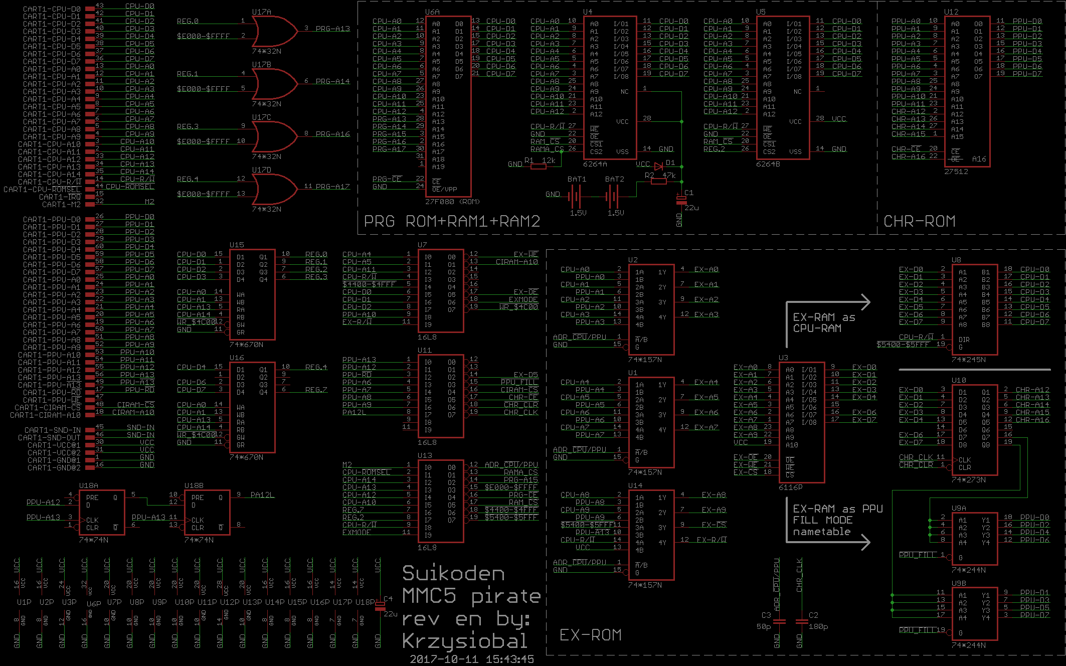
Here are PAL details and mapper description I did so far
Code:
U13:
ADR_!CPU!/PPU = (!EXMODE&!M2) | (!EXMODE&!CPU-!ROMSEL!) | (!EXMODE&!CPU-A14) | (!EXMODE&!CPU-A12) | (!EXMODE&!CPU-A10) | (!EXMODE&CPU-R/!W!) | (!EXMODE&CPU-A13);
In VHDL:
ADR_!CPU!/PPU <= '0' when EXMODE='0' and CPU-R/!W!='0' and CPU-A10='1' and CPU-A12='1' and CPU-A13='0' and CPU-A14='1' and CPU-!ROMSEL!='1' and M2='1' else --cpu write at $5400-$5fff
'0' when EXMODE='1' else
'1';
RAMA_CS = (!REG.2);
In VHDL:
RAMA_CS <= not REG.2;
PRG-A15 = (CPU-A13&CPU-A14) | (REG.2);
In VHDL:
PRG-A15 <= (CPU-A13 and CPU-A14) or (REG.2);
$E000-$FFFF = (CPU-A13&CPU-A14);
In VHDL:
$E000-$FFFF <= '1' when CPU-A13='1' and CPU-A14='1' else '0'
PRG-!CE! = (!REG.7&!CPU-A14) | (CPU-!ROMSEL!);
In VHDL:
PRG-!CE! <= '1' when REG.7='0' and CPU-A14='0' else CPU-!ROMSEL!;
RAM_!CS! = (!CPU-A13&CPU-!ROMSEL!) | (REG.7&!CPU-!ROMSEL!) | (CPU-!ROMSEL!&!M2) | (CPU-A14&!CPU-!ROMSEL!) | (!CPU-A14&CPU-!ROMSEL!);
In VHDL:
RAM_!CS! <= '0' when CPU-A13='1' AND CPU-A14='1' AND CPU-!ROMSEL='1' AND M2='1' else
'0' when REG.7='0' AND CPU-A14='0' and CPU-!ROMSEL!='0' else
'1'
REG.7 | CPU-A13 | CPU-A14 | CPU-!ROMSEL! | M2 || RAM_!CS! |
0 | 0 | 0 | 0 | 0 || 0 | <--- 8000$-$bfff and REG.7=0
0 | 0 | 0 | 0 | 1 || 0 | <--- 8000$-$bfff and REG.7=0
0 | 1 | 0 | 0 | 0 || 0 | <--- 8000$-$bfff and REG.7=0
0 | 1 | 0 | 0 | 1 || 0 | <--- 8000$-$bfff and REG.7=0
0 | 1 | 1 | 1 | 1 || 0 | <-6000-$7fff
1 | 1 | 1 | 1 | 1 || 0 | <-6000-$7fff
!$4400-$4FFF! = (!M2) | (!CPU-!ROMSEL!) | (!CPU-A14) | (!CPU-A10) | (CPU-A12) | (CPU-A13);
In VHDL:
!$4400-$4FFF! <= '0' when M2='1' and CPU-!ROMSEL!='1' and CPU-A14='1' and CPU-A10='1' and CPU-A12='0' and CPU-A13='0' else '1';
!$5400-$5FFF! = (!M2) | (!CPU-!ROMSEL!) | (!CPU-A14) | (!CPU-A12) | (!CPU-A10) | (CPU-A13);
In VHDL:
!$5400-$5FFF! <= '0' when M2='1' and CPU-!ROMSEL!='1' and CPU-A14='1' and CPU_A12='1' and CPU-A10='1' and CPU=A13=0 else '1';
--------------------------------------------------------------------------------------------
U11:
O0 = (!I8);
In VHDL:
O0 <= not I8; --but it is unwired
O1 = (I11); --so O1 acts as an input but seems to not have influence to any output)
EX-D5 = (PA12L & PPU-!RD! & !PPU-A13);
In VHDL:
EX-D5 <= '1' when PA12L='1' and PPU-!RD!='1' and PPU-A13='0' else '0'
!PPU_FILL! = (!PPU-A13) | (!PPU-A6) | (!PPU-A7) | (!PPU-A8) | (!PPU-A9) | (PPU-!RD!);
In VHDL:
!PPU_FILL! <= (not PPU-A13) or (not PPU-A6) or (not PPU-A7) or (not PPU-A8) or (not PPU-A9) or (PPU-!RD!);
CIRAM-!CS! = (PPU-A9 & PPU-A8 & PPU-A7 & PPU-A6 & !PPU-!RD!) | (!PPU-A13);
In VHDL:
CIRAM-!CS! <= (PPU-A9 and PPU-A8 and PPU-A7 and PPU-A6 and !PPU-!RD!) or (not PPU-A13);
CHR-!CE! = (PPU-!RD!) | (PPU-A13);
In VHDL:
CHR-!CE! <= (PPU-!RD!) or (PPU-A13);
!CHR_CLR! = (PPU-A12) | (PPU-A13);
In VHDL:
!CHR_CLR! <= (PPU-A12) or (PPU-A13);
CHR_CLK = (PPU-!RD!&PPU-A13);
In VHDL:
CHR_CLK <= (PPU-!RD! and PPU-A13);
--------------------------------------------------------------------------------------------
U7:
EX-!WE! = (EX-R/!W/) | (CPU-R/!W!);
In VHDL:
EX-!WE! <= (EX-R/!W/) or (CPU-R/!W!);
CIRAM-A10 = Non-combinatorial
O2 = Non-combinatorial
O3 = Non-combinatorial
O4 = Non-combinatorial
EX-!OE! = Non-combinatorial
EXMODE = Non-combinatorial
In VHDL:
O2 <= D0 when CPU-A5='1' and CPU-A4='0' and CPU-A11='1' and CPU-R/!W!='0' and !$4400-$4FFF!='0'; //latch
O3 <= D2 when CPU-A5='1' and CPU-A4='0' and CPU-A11='1' and CPU-R/!W!='0' and !$4400-$4FFF!='0'; //latch
O4 <= D0 when CPU-A5='1' and CPU-A4='1' and CPU-A11='1' and CPU-R/!W!='0' and !$4400-$4FFF!='0'; //latch
EXMODE <= D1 when CPU-A5='1' and CPU-A4='1' and CPU-A11='1' and CPU-R/!W!='0' and !$4400-$4FFF!='0'; //latch
EX-!OE! <= not (EXMODE or O4)
CIRAM-A10 <= '0' when O3='0' and O2='0' else
not PPU-A10 when O3='0' and O2='1' else
PPU-A10 when O3='1' and O2='0' else
'1';
!WR_$4C00! = (!CPU-A11) | (!$4400-$4FFF!) | (CPU-R/!W!) | (CPU-A5) | (CPU-A4); !WR_$4C00! , mask: $FC30
In VHDL:
!WR_$4C00! <= (not CPU-A11) or (!$4400-$4FFF!) or (CPU-R/!W!) or (CPU-A5) or (CPU-A4); !WR_$4C00! , mask: $FC30
Those latched regs summary:
$4c00 .... .... (no effect?)
$4c10 .... .... (no effect?)
$4c20 .... .m.m
| |
+++-- mirroring (source of CIR10): 0: GND, 1: not PA10, 2: PA10, 3: VCC
$4c30 .... ..ee
||
++-- value of EX-!OE! to be latched (enable reading from EX-ram: 0=disable=VCC, 1..3:enable=GND)
+--- value of EXMODE to be latched
--------------------------------------------------------------------
Hardware: 256K PRG-ROM
8KB PRG-RAM battery backed (6264A)
8KB PRG-RAM not backed (6264B)
64KB CHR-ROM
1KB EX-RAM (can be used by CPU & PPU)
Quirks:
* Data bit 5 of EX-RAM is not wired to anything
CPU memory map:
$4400-$47ff: registers
$4c00-$4fff: registers (mirror)
PPU memory map:
$0000-$0fff: 4KB CHR-ROM bank
$1000-$1fff: 4KB CHR-ROM bank
0b1xxx1111xxxxxx: fill mode
$5400-$57ff: EXRAM
$5c00-$5fff: EXRAM (mirror)
$6000-$7fff: RAM (controlled by $4c03)
$8000-$9fff: ROM or RAM (controlled by $4c00)
$a000-$bfff: ROM or RAM (controlled by $4c01)
$c000-$dfff: ROM (controlled by $4c02)
$e000-$ffff: ROM (hardwired to last bank)
[r..p pppp] $4c00 (mask: $fc33)
| | ||||
| +-++++- select 8kB ROM bank at $8000-$9fff (ignored when RAM is selected)
| +--- select RAM chip 0=6264A, 1=6264B (ignored when ROM is selected)
+--------- 0: select RAM, 1:select ROM
[r..p pppp] $4c01 (mask: $fc33)
| | ||||
| +-++++- select 8kB ROM bank at $a000-$bfff (ignored when RAM is selected)
| +--- select RAM chip 0=6264A, 1=6264B (ignored when ROM is selected)
+--------- 0: select RAM, 1:select ROM
[...p pppp] $4c02 (mask: $fc33)
| ||||
+-++++- select 8kB ROM bank at $c000-$dfff
[.... .p..] $4c03 (mask: $fc33)
|
+--- select RAM chip for $6000-$7fff: 0=6264A, 1=6264B
[.... .m.m] $4c20 (mask: $fc30)
| |
+++-- Mirroring - source of CIRAM-A10: 0=GND, 1=not PA10, 2=PA10, 3=VCC
[.... ..ee] $4c30 (mask: $fc30)
||
++-- controls EX-RAM !OE line (0:disable, 1..3:enable)
+--- controls what is connected to EX-RAM address bus,!WE and !CS:
0=CPU bus when CPU writes at $5400-$57ff/$5c00-$5fff, otherwise PPU bus)
1=always CPU bus
EX-RAM behaviour:
CPU has two windows ($5400-$57ff and $5c00-$5fff) to read/write to EX-RAM memory.
The behaviour of EX-RAM depends of how $4c30 bits are set.
CPU can always write to EX RAM (and those write cycles have priority over any other EXRAM activity)
0: reading from EXRAM (by CPU/PPU) returns open bus; CPU can write to EX-RAM.
1: reading EXRAM by CPU returns open bus; CPU can write to EX-RAM; PPU can read EX-RAM
2-3: CPU can read & write to EX-RAM, PPU cannot read from it.
