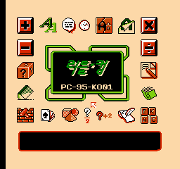
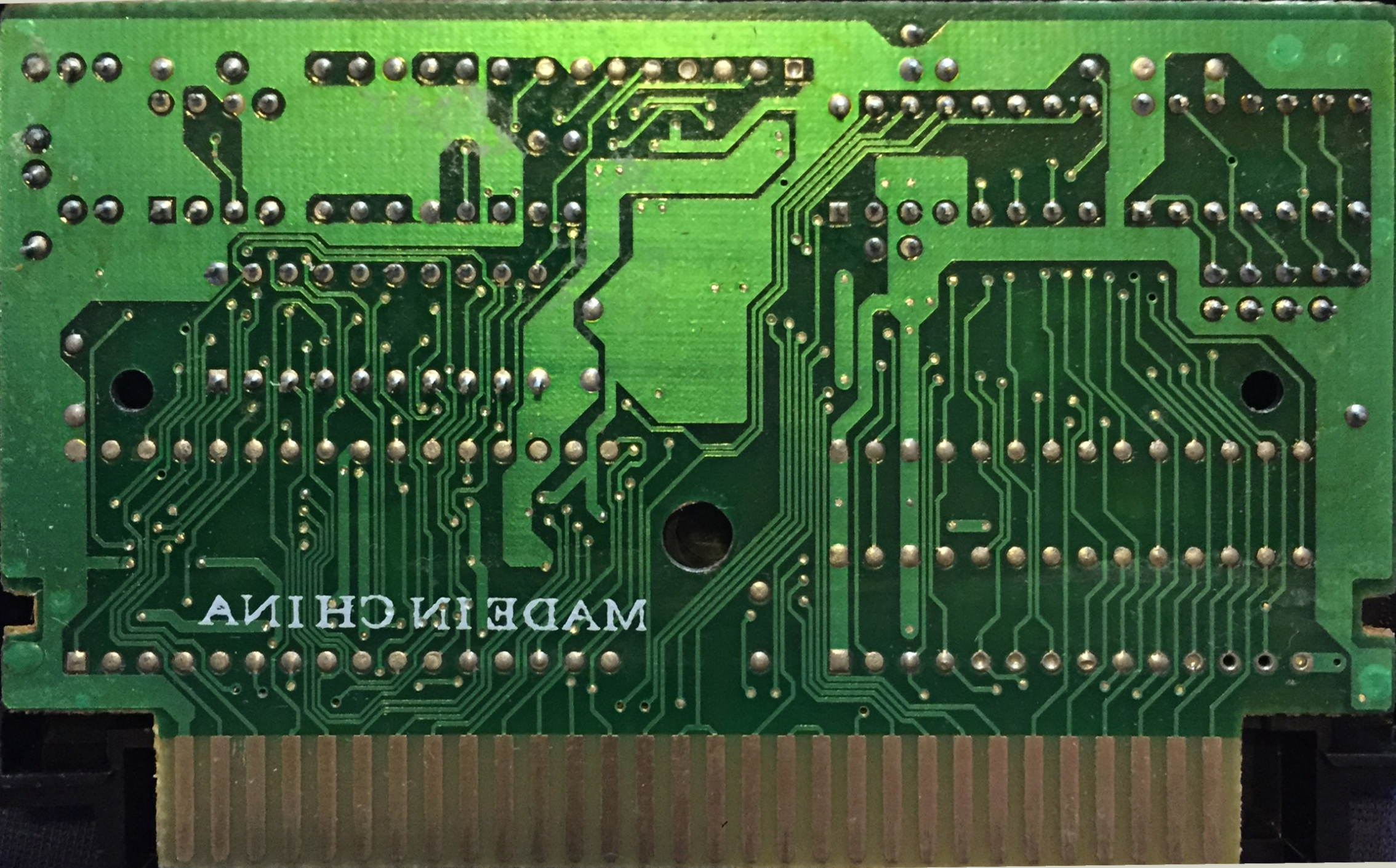
I have this this weird cartridge for quite long time (called Asder PC 95):
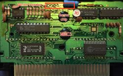

It looks like some add-on cartridge for those keyboard famiclones, mainly designed for learning English language (everything is about guessing words)
Brief analysis has shown that the cartridge might have additional audio channels (audio lines are wired to some mysterious chips)So let's reverse engineer it:
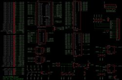
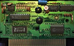
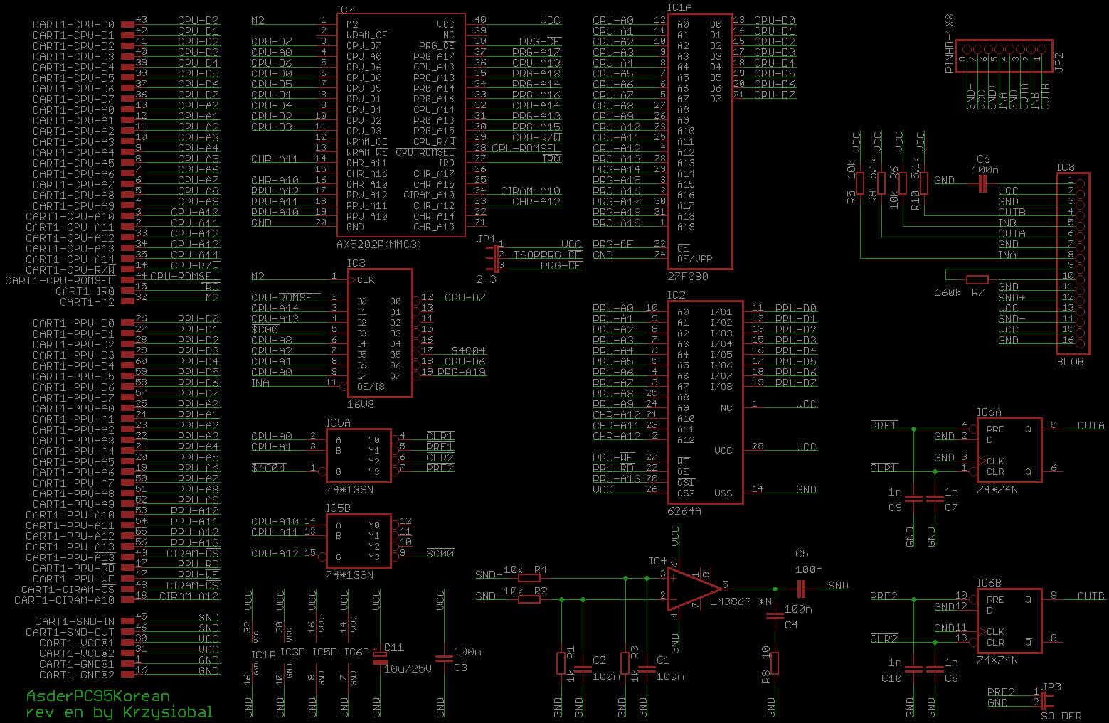
There is 1MB PRG-ROM, 8kB CHR-RAM, Mapper blob chip (which seems to be MMC3 with exact pinout (ommiting WRAM and CHR-A13..A17 lines), second mysterious blob, opamp, 7474, and PAL16V8.
PAL is read-protected but I was able to deduct its functionality after analyzing its behaviour.
So except the ordinary MMC3 registers ($8000-$ffff), there are a few others coming from the PAL:
For pedantics:
* $c000 and $e000 always point to the last outer PRG-bank selected
* Those bits does not take into account if MMC3 is configured in swap-PRG mode ($8000.6=1)
* After writing value to $8001, game code writes the same value to $4c00 when $8000=#6. Same wieth $4c01 when $8000=#7. So it can be emulated as oversided (1MB) MMC3.
* Hardware logic does not not distinguish between read and write cycle for above registers, so when writing into a readable reg - bus conflict occurs and when reading from writable reg - actual written data will be unknown (due to open bus behaviour, probably high byte of the opcode)
* CHR-RAM A10..A12 is controlled by MMC3.
INA/INB seems to be inputs (due to pulled-ups to VCC)
OUTA/OUTB seems to be general purpose output pins for generating arbitrary waveforms so I called them that way (they're also pulled to VCC for unknown reason)
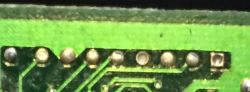
Mysterious BLOB chip and unpopulated 8-pin header:
There is a unknown blob chip with the following lines wired into the die:
There are also unpopulated 8 pins which are not only vias, but also seems to create some kind of header-connector for connecting unknown peripheral (note square shape for determining first pin)
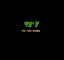
I found ROM called `ASDER PC-95 (16-in-1) (Arab)` which has quite different menu items and music varies. Also it is only 512 kB. Arab version is controlled using Subor Keyboard.


However, the Korean one described in this topic does not respond to joypad nor Subor Keyboard (game does not even poll $4016/$4017). Later I found out that it writes/reads to a bunch of another registers every frame, which seems to be designed for communicating with keyboard.
So it looks like $4900 is used for distinguishing between different version of registers used for keyboards communication.
There is 11 (or 12 byte) keyboard buffer. Value written to $491f (or $4904) sets pointer to desider address of the buffer and
reading from $491f (or $4906) returns its value.
Keyboard layout:
I started by guessing which bits are responsible for up/down/left/right and return. Then I looked at the Subor's keyboard layout and found it to be similar. Then I applied it to the game logic and at least the following keys work: letters, numbers, space, return, arrows, backspace, delete.
What is to be examined:
1)
Register $4C03.7:
This is also unknown use. Game every frame makes such loop:
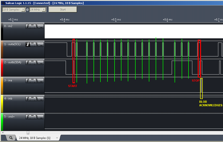
If the returned bit is set, game does not respond on clicking any position in the menu. My guess is that those OUTA/OUTB are used as clock/data for some external input device (yet another version of keyboard?), while $4c03.7 is like ready/busy signal and one of the INA/INB is used as data signal from the device to the cartridge.
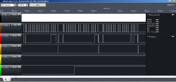
2) How to stimulate the glob to generate some audio (by OUTA/OUTB/INA/INB lines). Measuring on scope both sides of the 160k resistor shows no signal, so maybe it is defected? Or it is the kind of chip, used for generating pre-programmed sounds that only generate clock while playing sound?)
This is waveform on those lines after powerup:
3) What external peripheral can be connected to the unknown header and what is the protocol
4) I started data/code logging in FCEUX, clicked every position in the menu and played the game for quite long time but is shows only about 3% of code executed and 7% of data used. Looking at the non-used portions of ROM shows something that looks either as random or compressed. 1024 kB of game and only 10% of code/data is used? Weird that this game is 2 times bigger than the Arabic version but it does not even have a text editor.
---
ROM:
https://drive.google.com/file/d/1iBb5vE ... jQMOR/view


It looks like some add-on cartridge for those keyboard famiclones, mainly designed for learning English language (everything is about guessing words)
Brief analysis has shown that the cartridge might have additional audio channels (audio lines are wired to some mysterious chips)So let's reverse engineer it:
There is 1MB PRG-ROM, 8kB CHR-RAM, Mapper blob chip (which seems to be MMC3 with exact pinout (ommiting WRAM and CHR-A13..A17 lines), second mysterious blob, opamp, 7474, and PAL16V8.
PAL is read-protected but I was able to deduct its functionality after analyzing its behaviour.
Code:
n4C04 <= (!M2) | (!CPU_nROMSEL) | (!CPU_A14) | (!CPU-A2) | (CPU_A8) | (nC00) | (CPU_A13);
O4 <= D6 when M2 & nROMSEl & A14 & !A13 & !nC00 & !A8 & !A2 & !A1 & A0
O2 <= this line behaves weird, seems to be some helper line for the above latch
O3 <= D6 when M2 & nROMSEl & A14 & !A13 & !nC00 & !A8 & !A2 & !A1 & !A0
O1 <= this line behaves weird, seems to be some helper line for the above latch
D7 <= INA when M2 & nROMSEl & A14 & !A13 & !nC00 & !A8 & !A2 & A1 & A0 else 'Z'
PRG_A19 <= O3 when !CPU_A14 & !CPU_A13 else
O4 when !CPU_A14 & CPU_A13 else
'1'
So except the ordinary MMC3 registers ($8000-$ffff), there are a few others coming from the PAL:
Code:
Mask: $fd07
$4C00 (w): [.P.. ....] - sets outer 512 kB PRG-bank for $8000
$4C01 (w): [.P.. ....] - sets outer 512 kB PRG-bank for $a000
$4C02 - nothing
$4C03 (r): [I... ....] - I=value of INA pin, .=OPEN BUS
$4c04 (w): [.... ....] - outputs 0 on OUTA
$4c05 (w): [.... ....] - outputs 1 on OUTA
$4c06 (w): [.... ....] - outputs 0 on OUTB
$4c07 (w): [.... ....] - outputs 1 on OUTB
For pedantics:
* $c000 and $e000 always point to the last outer PRG-bank selected
* Those bits does not take into account if MMC3 is configured in swap-PRG mode ($8000.6=1)
* After writing value to $8001, game code writes the same value to $4c00 when $8000=#6. Same wieth $4c01 when $8000=#7. So it can be emulated as oversided (1MB) MMC3.
* Hardware logic does not not distinguish between read and write cycle for above registers, so when writing into a readable reg - bus conflict occurs and when reading from writable reg - actual written data will be unknown (due to open bus behaviour, probably high byte of the opcode)
* CHR-RAM A10..A12 is controlled by MMC3.
INA/INB seems to be inputs (due to pulled-ups to VCC)
OUTA/OUTB seems to be general purpose output pins for generating arbitrary waveforms so I called them that way (they're also pulled to VCC for unknown reason)
Mysterious BLOB chip and unpopulated 8-pin header:
There is a unknown blob chip with the following lines wired into the die:
Code:
01 02 03 04 05 06 07 08 09 10 11 12 13 14 15 16
100nF VCC GND OUTB INB OUTA GND INA | | GND SND+ VCC SND- VCC GND
to GND +-160k-+
reset? clock generator?
100nF VCC GND OUTB INB OUTA GND INA | | GND SND+ VCC SND- VCC GND
to GND +-160k-+
reset? clock generator?
There are also unpopulated 8 pins which are not only vias, but also seems to create some kind of header-connector for connecting unknown peripheral (note square shape for determining first pin)

Code:
SND- VCC SND+ INA GND OUTA INB OUTB
I found ROM called `ASDER PC-95 (16-in-1) (Arab)` which has quite different menu items and music varies. Also it is only 512 kB. Arab version is controlled using Subor Keyboard.


However, the Korean one described in this topic does not respond to joypad nor Subor Keyboard (game does not even poll $4016/$4017). Later I found out that it writes/reads to a bunch of another registers every frame, which seems to be designed for communicating with keyboard.
Code:
read $4900;
+------equals #$e6?---------+
| yes |no
\./ \./
$491f <- #$00 | $4904 <- #$00
$491f -> read | $4906 -> read
$491f <- #$01 | $4904 <- #$01
$491f -> read | $4906 -> read
... | ...
$491f <- #$0a | $4904 <- #$0a
$491f -> read | $4906 -> read
| $4904 <- #$0b
| $4906 -> read
|
$4905 <- #$82 | $4905 <- #$82
...
depending on values read from $491f/$4906
only FFs -> the code polls joypad
only 00s -> the code doesn't poll joypad
So it looks like $4900 is used for distinguishing between different version of registers used for keyboards communication.
There is 11 (or 12 byte) keyboard buffer. Value written to $491f (or $4904) sets pointer to desider address of the buffer and
reading from $491f (or $4906) returns its value.
Keyboard layout:
I started by guessing which bits are responsible for up/down/left/right and return. Then I looked at the Subor's keyboard layout and found it to be similar. Then I applied it to the game logic and at least the following keys work: letters, numbers, space, return, arrows, backspace, delete.
Code:
----------------bits (0=key pressed, 1 = key not pressed)------------------------------
----7---- ----6---- ----5---- ----4---- ----3---- ----2---- ----1---- ----0----
-$0-- V 5 E F2 C F G 4
-$1-- X 3 W F1 END S D 2
-$2-- HOME DELETE PRIOR F8 RIGHT NEXT BACK INSERT
-$3-- PERIOD 0 6 F5 COMMA L I 9
-$4-- DOWN BACKSLASH LBRACKET F7 LEFT UP RETURN RBRACKET
-$5-- LCONTROL 1 A ESCAPE TAB Z CAPITAL Q
-$6-- J 8 U F4 M K Y 7
-$7-- LSHIFT EQUALS P F6 SLASH APOSTROPHE SEMICOLON MINUS
-$8-- B 6 R F3 SPACE N H T
-$9-- NUMPAD2 NUMPAD8 NUMPAD4 GRETURN NUMPAD6
-$10- NUMPAD8 NUMPAD2 NUMPAD1 F12 F11 NUMPAD7 NUMPAD4 LMENU
-$0a- NUMLOCK DIVIDE NUMPAD5 F10 NUMPAD9 MULTIPLY ADD SUBTRACT
-$0b- NUMPAD0 DECIMAL NUMPAD3 F9 SPACE PAUSE NUMPAD6 GRAVE
What is to be examined:
1)
Register $4C03.7:
This is also unknown use. Game every frame makes such loop:
Code:
3F:E39F: AD 03 4C LDA $4C03 = #$FF
3F:E3A2: 29 80 AND #$80
3F:E3A4: D0 F9 BNE $E39F
3F:E3A2: 29 80 AND #$80
3F:E3A4: D0 F9 BNE $E39F
If the returned bit is set, game does not respond on clicking any position in the menu. My guess is that those OUTA/OUTB are used as clock/data for some external input device (yet another version of keyboard?), while $4c03.7 is like ready/busy signal and one of the INA/INB is used as data signal from the device to the cartridge.
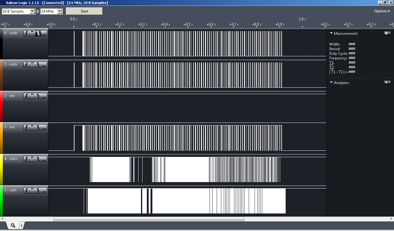
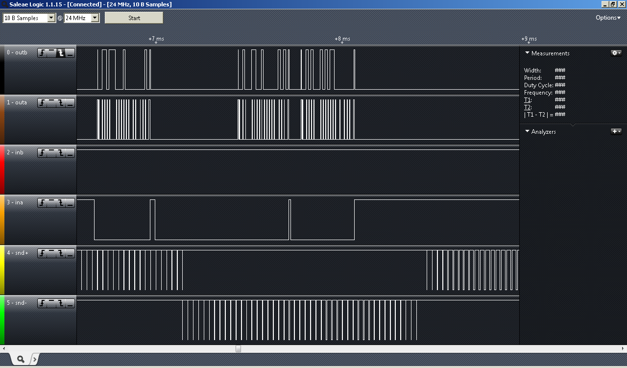
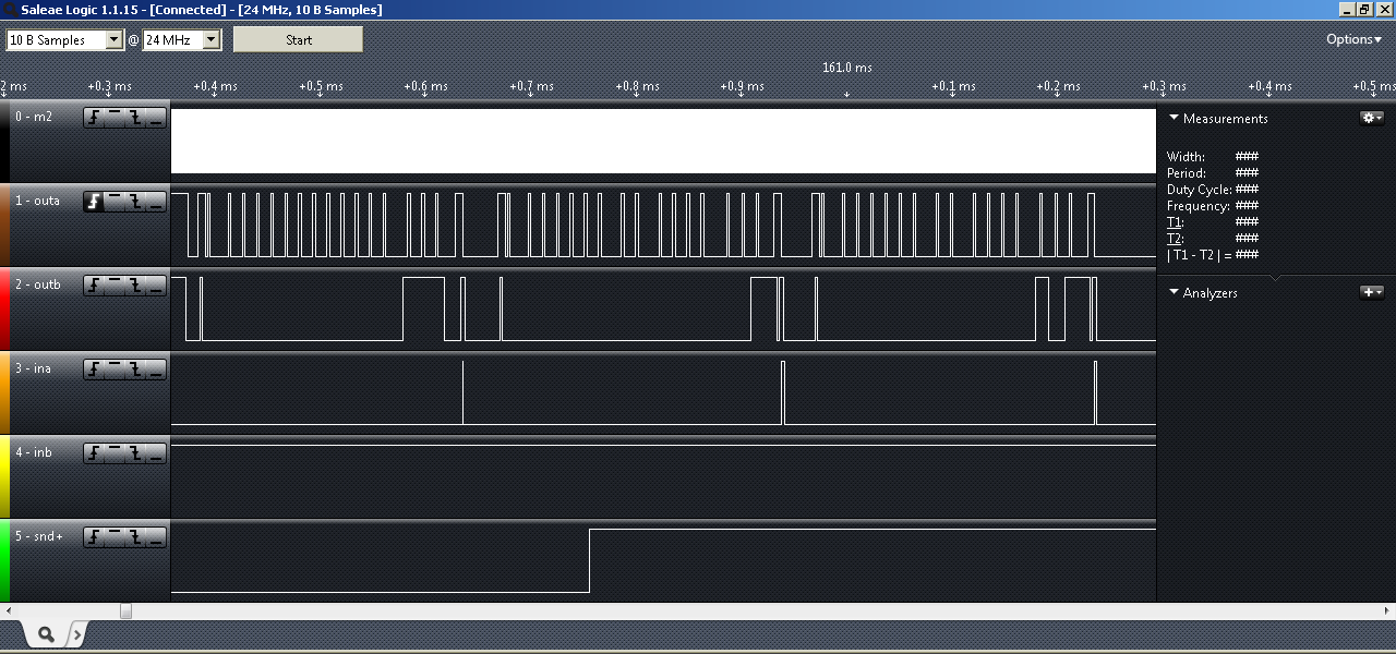
2) How to stimulate the glob to generate some audio (by OUTA/OUTB/INA/INB lines). Measuring on scope both sides of the 160k resistor shows no signal, so maybe it is defected? Or it is the kind of chip, used for generating pre-programmed sounds that only generate clock while playing sound?)
This is waveform on those lines after powerup:
3) What external peripheral can be connected to the unknown header and what is the protocol
4) I started data/code logging in FCEUX, clicked every position in the menu and played the game for quite long time but is shows only about 3% of code executed and 7% of data used. Looking at the non-used portions of ROM shows something that looks either as random or compressed. 1024 kB of game and only 10% of code/data is used? Weird that this game is 2 times bigger than the Arabic version but it does not even have a text editor.
---
ROM:
https://drive.google.com/file/d/1iBb5vE ... jQMOR/view