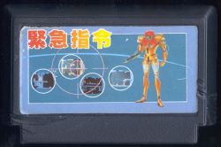
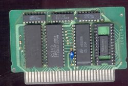
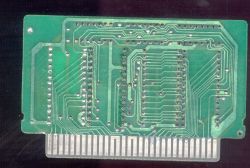
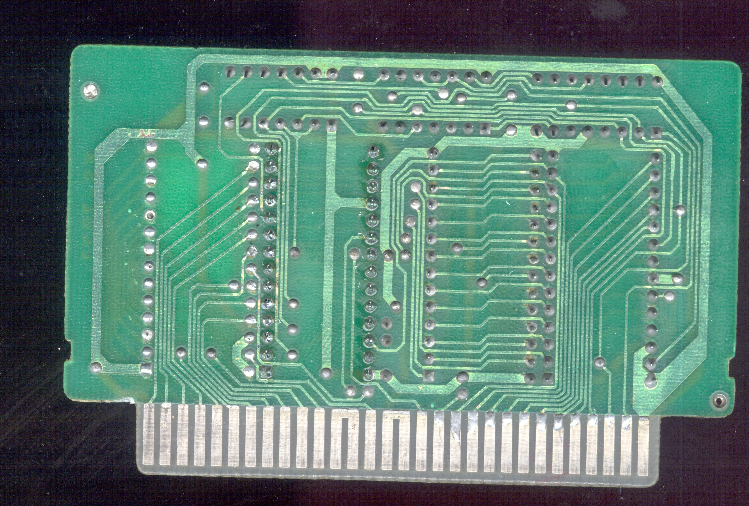
I finally was able to obtain one game with KS 204 Kaiser chip and analyze it.
The KS204 chip is nothing more but a Kaiser clone of Tengen MIMIC-1 MMC3 predessor (INES Mapper 206), known also as NTDEC 8701.
The only difference is lack of PRG/CE pin (instead, external RESET is present) and shuffled pinout.
Details:
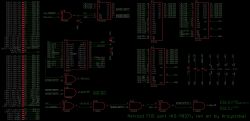
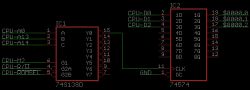
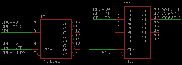
* Latching values into registers occurs on the rising edge of its decoding signal, for example register $8000 has decoding signal like:
CLK <= '0' when /ROMSEL = 0 and M2 = 1 and R/W = 0 and A1 = 0 and A14 = 0 and A13 = 0 else '1'
This can be precisely simulated using 74138+74574:
* PRG bank address lines does not take CPU-!ROMSEL into account so $0000-$7fff mirrors $8000-$ffff (important when external logic enables ROM under $8000)
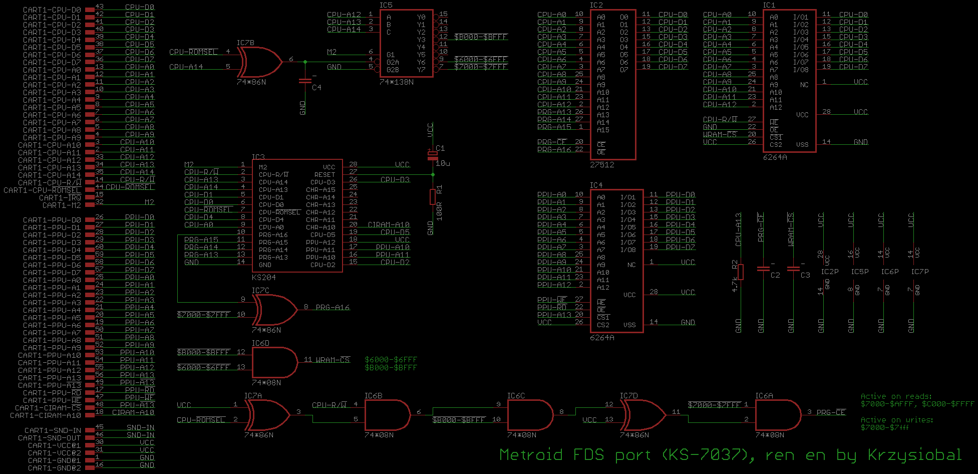
However, the "Metroid [FDS port], PCB: KS-7037)" games that uses it, connects it differently, which results in the following register order:

The KS204 chip is nothing more but a Kaiser clone of Tengen MIMIC-1 MMC3 predessor (INES Mapper 206), known also as NTDEC 8701.
The only difference is lack of PRG/CE pin (instead, external RESET is present) and shuffled pinout.
Code:
.--\/--.
M2 -> |01 28| -- +5V
CPU R/!W -> |02 27| <- RESET
CPU A14 -> |03 26| <- CPU D3
CPU A13 -> |04 25| -> CHR A15
CPU D1 -> |05 24| -> CHR A14
CPU D0 -> |06 23| -> CHR A13
CPU !RMS -> |07 22| -> CHR A12
CPU D4 -> |08 21| -> CHR A11
CPU A0 -> |09 20| -> CHR A10
PRG A16 <- |10 19| <- CPU D5
PRG A15 <- |11 18| <- PPU A12
PRG A14 <- |12 17| <- PPU A11
PRG A13 <- |13 16| <- PPU A10
GND -- |14 15| <- CPU D2
`------'
KS 204
Details:
* Latching values into registers occurs on the rising edge of its decoding signal, for example register $8000 has decoding signal like:
CLK <= '0' when /ROMSEL = 0 and M2 = 1 and R/W = 0 and A1 = 0 and A14 = 0 and A13 = 0 else '1'
This can be precisely simulated using 74138+74574:
* PRG bank address lines does not take CPU-!ROMSEL into account so $0000-$7fff mirrors $8000-$ffff (important when external logic enables ROM under $8000)
However, the "Metroid [FDS port], PCB: KS-7037)" games that uses it, connects it differently, which results in the following register order:
Code:
$8000.R2 [.......I] - nametable for $2000
$8000.R3 [.......J] - nametable for $2800
$8000.R4 [.......K] - nametable for $2400
$8000.R5 [.......L] - nametable for $2c00
$8001.R6 [....ABCD]
$8001.R7 [....EFGH]
$6000 $7000 $8000 $9000 $a000 $b000 $c000 $d000 $e000 $f000
----- ----- ----- ----- ----- ----- ----- ----- ----- -----
RAM ROM ROM ROM ROM RAM ROM ROM ROM ROM
0 11111 ABCD0 ABCD1 01100 1 EFGH0 EFGH1 01110 01111 <- 4 kiB Bank
^ ^ ^ ^
+-----+-----------------+-----+------------------- those bits are inverted
Writing to $7000-$7fff can cause bus-conflicts (ROM is enabled at that region during writes),
while writing to other regions doesn't.
The UNL-KS7037 FCEUX mapper implementation does not invert those bits but that's because
my implementation respects the PRG-A16 address line (just like the EPROM was dumped first and then
mapper was implemented to match it)