While investigating why WRAM emulation in
Best Play Pro Yakyuu Special wouldn't work properly, Pongbashi and I found that the cartridge uses a rather unique board labeled
SXROM. I've never heard of this board before so I thought it would be interesting to post about it here.
PCB shots by Pongbashi:
http://nestopia.netfast.org/mmc1.html
It differs from other MMC1 based boards with 16K WRAM (SOROM,SVROM?) in that the
lower three bits of register 1 (CHR0) appear to control WRAM banking. The game always set it to $7 for upper bank select and $0 for lower bank select, although perhaps only the first bit is what matters.
Emulation related:
Since the game needs special treatment for full WRAM emulation, this board should be a good sub-mapper candidate for iNES 2.0.

Edit: Spoke too soon. Looking up
62256 revealed that this is a
32K WRAM(!) cart and not 16K.
It would not be bit 0 that controls the WRAM bank, since that bit doesn't get output by the MMC1 in 8K mode. It would have to be either bit 1 or bit 2 that controls the bankswitching.
Marty wrote:
While investigating why WRAM emulation in
Best Play Pro Yakyuu Special wouldn't work properly, Pongbashi and I found that the cartridge uses a rather unique board labeled
SXROM. I've never heard of this board before so I thought it would be interesting to post about it here.
PCB shots by Pongbashi:
http://nestopia.netfast.org/mmc1.htmlIt differs from other MMC1 based boards with 16K WRAM (SOROM,SVROM?) in that the
lower three bits of register 1 (CHR0) appear to control WRAM banking. The game always set it to $7 for upper bank select and $0 for lower bank select, although perhaps only the first bit is what matters.
Emulation related:
Since the game needs special treatment for full WRAM emulation, this board should be a good sub-mapper candidate for iNES 2.0.
Edit: Spoke too soon. Looking up
62256 revealed that this is a
32K WRAM(!) cart and not 16K.
There appears to be *32K* of RAM on that board, not just 16K. It could use different 8K sections for the various saved games. The RAM on the board is indeed a 62256 which is 32K bytes.
As for NES 2.0, I will add this to it. And speaking of that, I have about completed my NES 2.0 additional mappers and I have almost finished processing the ROMs/headers. I still need to work on the Vs. system stuff, but I'm a little hesitant since I don't have a complete set of boards yet. I just got Vs. TKO boxing so I will be able to reverse engineer its custom protection chip when I get that.
Ahh, in that case it's possible that both bits 1 and 2 of $A000 are meaningful here. Either that, or they used a 32KB chip with the MSB pulled low to make only 16KB accessible. Examining the MMC1's wiring should provide a more definite answer here (see if CHR A13 and/or A14 go to the SRAM chip).
If my unerstanding is right, the only difference between SXROM and SOROM is that SOROM allow 16kb of WAM, and SXROM 32kb, that has nothing to do with "Final Fantasy I&II" that has 16kb of WRAM and one more PRG select adress, right ?
A brief visual inspection shows CHR A14 and A15 leading toward the PRG RAM, and CHR A16 leading toward the CHR RAM chip. CHR A12 and A13 might lead underneath the PRG RAM as well, though I can't be certain since a bunch of signals come out from underneath the chip.
It would help to know the actual pin to pin connections to figure out exactly what's going on here.
Pongbashi has opened up a few
other MMC1 carts now.
Final Fantasy I & II being one of them, turned out to be an... <drum roll>... SXROM.
So, as my understanding, on a SXROM card :
CHR bit 4 controls upper 512kb PRG selection, and this affect the hardwired bank as well, making 2 different "hardwired" banks, the first at the end of the first 256k, and the second at the end of the second 256k, just like SUROM does.
SXROM also controls the upper lines of a 32kb WRAM chip via CHR bits 2 and 3, in 8kb banks, as opposed to SOROM, wich only control 2 8kb WRAM chips via CHR bit 4 (and only one is battery backed).
Also, by the way SVROM doesn't exist at all and is just a misreading of SUROM, wich has later be assumed to be a variant of SUROM supporting WRAM banking, wich obviously was a wrong assumption since this variant is SXROM.
By the way, eveyone should stop at once to say "SxROM", "TxROM", etc, to refer to the whole group of boards using the same mapper, because this obviously confuses everything with the SXROM board aknowledged.
All of this should be definitely confirmed and wikified.
I thought SOROM used bit 4 of $A000 for its SRAM banking - perhaps I'm mistaken though.
If CHR A14 and A15 go to SRAM, then that should correspond to bits 2-3 of $A000, not bits 1-2 as I was thinking. I suppose bit 4 could control 256K PRG segmentation like SUROM, leaving bit 1 the only unused bit (with bit 0 controlling CHR banking in 4K mode, as is the case for all MMC1 variants).
Sorry, those bits are confusing me. I've edited my old post to correct the information. Say if there is still something wrong.
OK, your post looks right now, at least to the extent I can make out from what is known. As stated earlier, an inspection on the individual pin connections should clear up any remaining issues with regard to this board type.
Incidentally, I took a peek at Final Fantasy I & II, and it appears to set the CHR bank register to either $00 or $18, depending on the game selected.
That means the game actually only uses banks 0 and 2 of its 32kb SRAM chip, if I understand things right.
OK, I've put most things on the Wiki.
Now, I guess something should be done to avoid confusion between SxROM and SXROM (that is, the whole set of 'S' board using MMC1 and the particular SXROM). The 'x' letter probably come from it is the most used algebra variable letter, and has been used to show the letter can vary in the whole section of MMC1 board, while the 'S' letter doesn't varry. While the case currently distinct both, I think somethiny better could come up. That implict make a lot of changes on the Wiki, and rename whole pages, so I cannot go on and just do it myself.
Sorry for triple-posting, but wait ...
Tokmaru's New thread made me wondering something :
The SOROM board has no inverter to handle both chips, but I assume the thing noted Q1 is a transistor in an uncomon package, and that it does the inversion.
However, the SXROM has a 74HC04 inverter and I really cannot see what it is used. Look like only 3 gates are used, because the 3 others seems just tied to either VCC or GND (cannot see well), and Nintendo always did that with unused gate on their board. The inverter is obvioulsy close to the 32kb RAM chip, so it would have to do something with it, but normally the adresses don't need to be inverted or anything. Does anybody have an idea ?
Is the inverter used as an inverting buffer to clean up the signal coming off the CHR address lines?
Well, I don't think so. All I can say is that at least ONE gate is used (on pins 1&2) and the output of pin 2 go to the pin 20 of the RAM, wich seem to be /CS. I cannot see what is input on pin 1. Also it don't see that there is any input to pin 3 and 5 (I'm unsure) and pin 9, 11 and 13 are grounded. All outputs have only tracks leading outise of the board, but I don't see any significant use of any other output than pin 2.
I looked at the MMC1 pinout on Kevtris' site, and the WRAM enable pin was labeled "WRAM CE" and not "WRAM /CE." I don't know if it's a typo or if the output is high for WRAM accesses. If it's the latter, then (assuming my understanding of the hardware is right) it would need to be inverted before entering the WRAM chip as /CS.
CE is high (8kB SRAMs have separate low and high enables). Presumably it would be safer during the startup state.
This is a shame, beacause this make the task to create a SXROM by modifing a standard SNROM a lot harder. Normally, you could just disolver the 64k SRAM chip and replace it with the 256k one, by changing a few connexions.
Looking at the chips pinout :
Code:
EDIT : Removed wrong pinout found somewhere random on the net.
Code:
05. SRAM (8KB) 6264 Pinout:
__ __
+5V |01\/28| +5V
A12 |02 27| /WE
A7 |03 26| NC
A6 |04 25| A8
A5 |05 24| A9
A4 |06 23| A11
A3 |07 22| /OE
A2 |08 21| A10
A1 |09 20| /CE
A0 |10 19| D7
D0 |11 18| D6
D1 |12 17| D5
D2 |13 16| D4
GND |14 15| D3
------
The only modifications would be pins 1, 18, 19, 20, 21 and 26, wich would be rather easy to do. However, to invert CE, that makes the modification somewhat trickier to do.
Since it is also easy to modify a SNROM board to get a SUROM equivalent of it (by just adding one or two wires from the normal SNROM modification needed to insert standard EPROMs), it would be easy to get a board to have amazing ROM and RAM size allowing big RPGs taking advantage of MMC1's capabilities.
the 62256 diagram there is wrong.
pins 22, 21, 20, 19, 18, 17 are incorrect.
it should be:
Code:
+--()--+
A14 | 1 28| VCC
A12 | 2 27| /WE
A7 | 3 26| A13
A6 | 4 25| A8
A5 | 5 24| A9
A4 | 6 23| A11
A3 | 7 22| /OE
A2 | 8 21| A10
A1 | 9 20| /CS
A0 |10 19| D7
D0 |11 18| D6
D1 |12 17| D5
D2 |13 16| D4
GND |14 15| D3
+------+
That makes the mod significantly easier: bend pins 1 and 26 of the 62256 straight to the side so they don't go into the board, and hook them to the logic gates/mapper chip, so it properly banks the memory. Other than those 2 pins all pins match. If the pin 26 trace on the board doesn't go anywhere you don't even need to bend it, though bending it to the side probably makes soldering on a wire much easier.
Lord Nightmare
P.S. DanSS got an FF1+2 board and mapped out the whole SXROM mapper hookup properly, he just hasn't added it to the wiki yet iirc.
Sorry to come up with a wrong pinout. It had teach me to not take any info found on the net as accurate regardless of where it comes.
Anyway, there is still a small problems : pin 23 of 6264 it teach to be 'NC' in what I've posted, but acutally is a secondary active high CS input, that the MMC1 seems to have used rather than the classical /CE of pin 20, wich I assume is tied low on normal MMC1 carts. This bad idea from Nintendo make our life harder when trying to rewire a normal cart to support 32kb chips, unless I'm totally misunderstanding something.
I assume you mean pin 26 and not 23 of the 6264...
This makes things slightly more interesting, since we need to 'sanitize' the pinout before using it:
Code:
board holes: 62256 pins:
<A13 source> 26
<A14 source> 1
1 N/C
2 2
3 3
... ...
19 19
20 N/C
21 21
22 22
... ...
25 25
26 20
27 27
28 28
that oughta do it. mod requires 3 wires, for <board A13> -> <62256 pin 26>, <board A14> -> <62256 pin 1>, <board /CE (pin 26)> -> <62256 pin 20>
Lord Nightmare
Quote:
I assume you mean pin 26 and not 23 of the 6264...
Raah, this annoy me. Why am I always writing stuff down wrong ?
Quote:
that oughta do it. mod requires 3 wires, for <board A13> -> <62256 pin 26>, <board A14> -> <62256 pin 1>, <board /CE (pin 26)> -> <62256 pin 20>
Yes. In SXROM case, "board A13" would be CHR A14, and "board A14" would be CHR A15. But what about "board /CE" ? This one doesn't exist, because the MMC1 doesn't output anything for pin 23 /CE, but only for pin 26 CE. So if you do it like you said, the WRAM will be enabled when the CPU acess ROM, but disabled when trying to acess RAM. That wouldn't work of course.
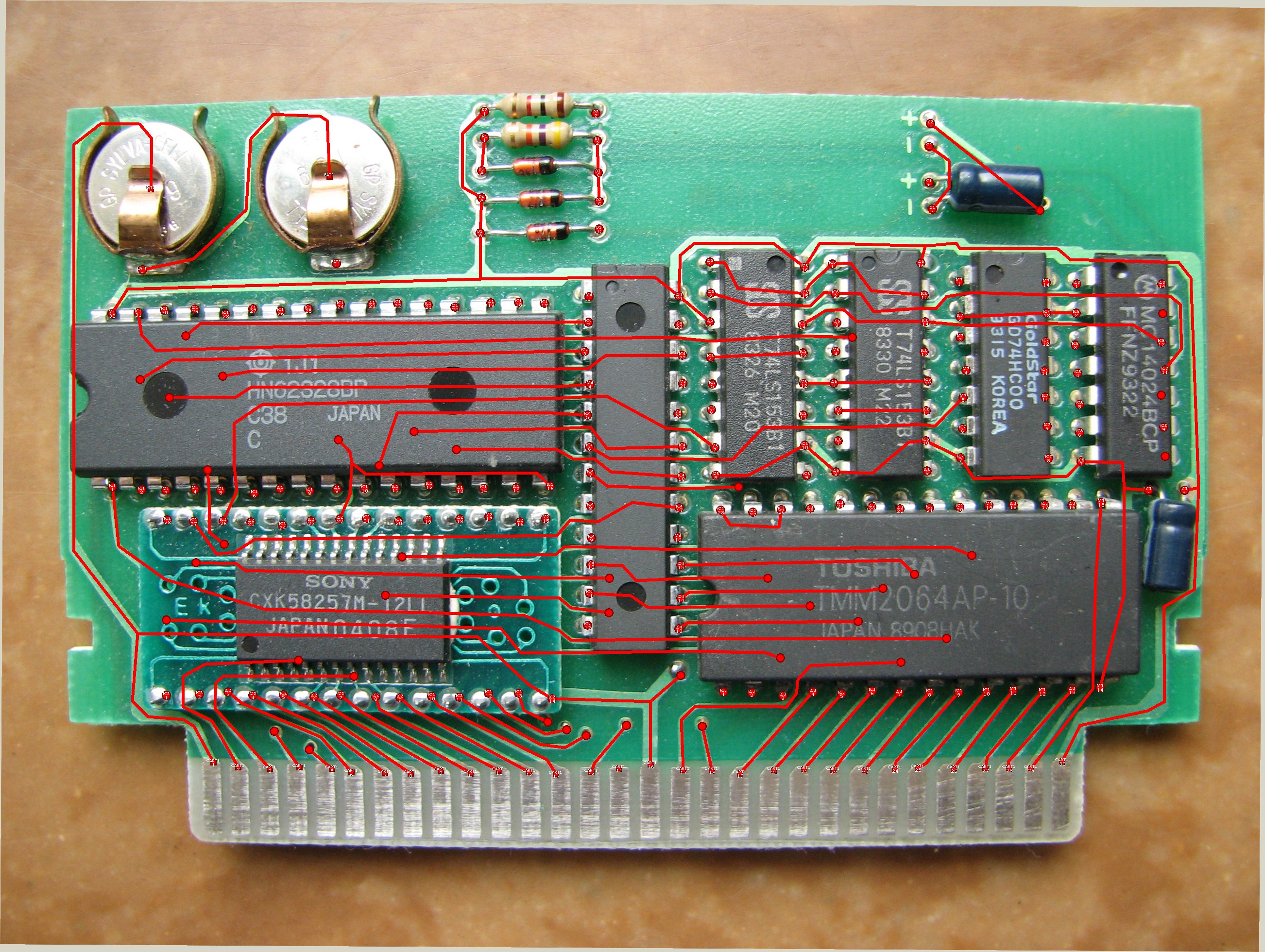
Quite interesting cartridge, they combined 3 MMC1 games into it, each of them using different PRG-ROM and PRG-RAM size.
Game switching occurs during reset, but it is not M2 based - they detect voltage drop (like in Atari 2600 multicarts) - 4024 is powered
from capacitor.
Each of game uses separate part of battery-backed RAM chip. Those 2x small 1.5V batts reminds me of the pirate MMC5 games. I don't know if they're recheargable, but there is 47k resistor which charges them when cartridge is powered from +5V.
74HC00 (used for inverting RAM-CE coming from MMC1) is also powered from batteries (that's why they used low power HC instead of LS).
Code:
Game | PRG-ROM | PRG-RAM | Link | ROM-A19 ROM-A18 | RAM-A14 RAM-A13
-----------------+---------+---------+----------------------------------------------------+-----------------+---------------
Sangokushi 256k 16k http://bootgod.dyndns.org:7777/profile.php?id=3170 | 0 0 | 0 *
Dragon Quest III 256k 8k http://bootgod.dyndns.org:7777/profile.php?id=1527 | 0 1 | 1 0
Dragon Quest IV 512k 8k http://bootgod.dyndns.org:7777/profile.php?id=1526 | 1 * | 1 1
I dump the cart with Kazzo (SOROM script). The first half of the PRG ROM was read (512kb) with DQ4(j). DQ4J ROM is identical to the original dump.