Hey everyone finally got around to making one of these and thought I would share how it is made.
Here is what you will need:
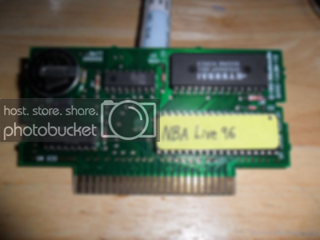
A 1A3M donor board
A 256k SRAM chip
A 32mbit TSOP chip
A switch with 3 leads
If you want to use the Reset button to switch between the games you can print up this board and use that instead of the switch.
http://nintendoage.com/forum/mess...
So lets get started.
Take your donor board and give it a test in the SNES to make sure it works.


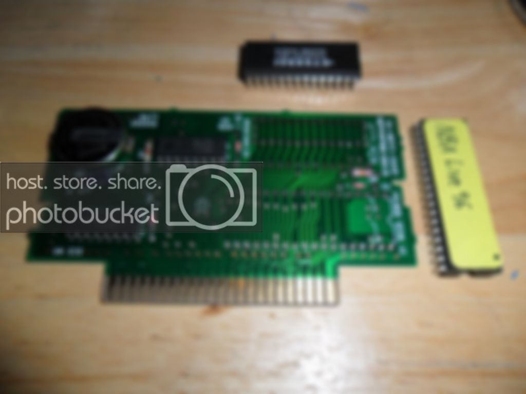
Next de-solder the mask ROM and SRAM chips
The SRAM must be upgraded so that each game can save progress

Now lets prepare the ROM for programming.
The GoW and PW ROMs are 1.5MB so they need to be expanded with Lunar Expand to 2MB (16mbit)
Or you can just download the XDelta patch at the bottom of the thread, you can apply it to a stock LTTP and it will patch the ROM and expand it to 16mbit, there is one for GoW and PWR both have a patch for a ROM with and without a copier header.
Once you have both of your ROMs ready open a command console by holding the shift key and and selecting open command window here

Next use the copy command with the binary flag to merge the 2 files together

Once the ROM is ready, go ahead and program it to a TSOP chip and mount it to a TSOP to DIP board

I like to give mine a test run in a board that I put a ZIF socket on before soldering it to the donor board

Now lets get the SRAM ready, here is the pinout for the 64k original SRAM and the new 256k SRAM that will be going in the board

Now we need 128k SRAM because both games use 64k to save looking at the pinout we only need to lift pin 26. Pin 1 can stay where it is, it will be connected to VCC and lock us to the upper half of the chip, this is fine because only 128k is needed anyway.
Now go ahead and bend up pin 26 on the SRAM, this will be connected to a switch to select between the 2 banks

Next you need to disconnect A21 on the mask ROM section so that it to can be conencted to the switch, I just followed the trace and made a cut in the PCB near one of the vias.

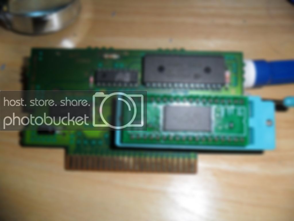
Now it is time to solder in the TSOP and SRAM, I started with the SRAM because it is shorter

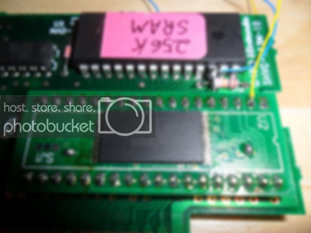
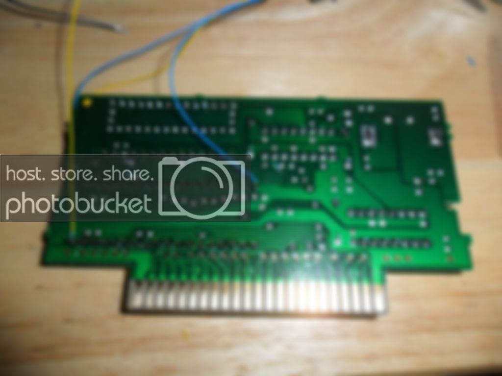
Once you have both the TSOP and SRAM installed connect a wire to pin 26 on the SRAM and pin 2 on the TSOP adapter board

Then connect a wire to VCC and ground anywhere on the board

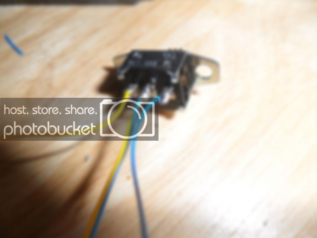
Now connect the 2 wires from the SRAM and the TSOP board to the center leg of the switch. VCC and ground will connect to the outer legs. This will force either all 0's or 1;s to these address lines and allow either game to load depending on where the switch is.

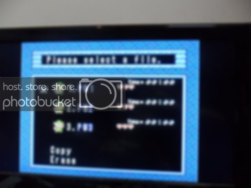
Now put it in the SNES and give it a test run, I made 3 saves to make sure that the SRAM was not being over wrote in the wrong spot on either game.

Then power off the SNES and flip the switch.
